SLVSCH9E December   2014  – March 2022 TPS62406-Q1 , TPS62407-Q1 , TPS62422-Q1 , TPS62423-Q1 , TPS62424-Q1

PRODUCTION DATA  

  1. Features
  2. Applications
  3. Description
  4. Revision History
  5. Device Comparison Table
  6. Pin Configuration and Functions
  7. Specifications
    1. 7.1 Absolute Maximum Ratings
    2. 7.2 ESD Ratings
    3. 7.3 Recommended Operating Conditions
    4. 7.4 Thermal Information
    5. 7.5 Electrical Characteristics
    6. 7.6 Timing Requirements
    7. 7.7 Switching Characteristics
    8. 7.8 Typical Characteristics
  8. Detailed Description
    1. 8.1 Overview
      1. 8.1.1 Converter 1
      2. 8.1.2 Converter 2
    2. 8.2 Functional Block Diagram
    3. 8.3 Feature Description
      1. 8.3.1 Enable
      2. 8.3.2 DEF_1 Pin Function
      3. 8.3.3 180° Out-of-Phase Operation
      4. 8.3.4 Short-Circuit Protection
      5. 8.3.5 Thermal Shutdown
      6. 8.3.6 EasyScale Interface: One-Pin Serial Interface for Dynamic Output-Voltage Adjustment
        1. 8.3.6.1 General
        2. 8.3.6.2 Protocol
    4. 8.4 Device Functional Modes
      1. 8.4.1 Power-Save Mode
        1. 8.4.1.1 Dynamic Voltage Positioning
        2. 8.4.1.2 Soft Start
        3. 8.4.1.3 100% Duty-Cycle Low-Dropout Operation
        4. 8.4.1.4 Undervoltage Lockout
      2. 8.4.2 Mode Selection
    5. 8.5 Programming
      1. 8.5.1 Addressable Registers
        1. 8.5.1.1 Bit Decoding
        2. 8.5.1.2 Acknowledge
        3. 8.5.1.3 Mode Selection
  9. Application and Implementation
    1. 9.1 Application Information
      1. 9.1.1 Application Information
    2. 9.2 Typical Application
      1. 9.2.1 Design Requirements
      2. 9.2.2 Detailed Design Procedure
        1. 9.2.2.1 Output Voltage Setting
          1. 9.2.2.1.1 Converter 1 Fixed Default Output-Voltage Setting
          2. 9.2.2.1.2 Converter 2 Fixed Default Output-Voltage Setting
        2. 9.2.2.2 Output Filter Design (Inductor and Output Capacitor)
          1. 9.2.2.2.1 Inductor Selection
          2. 9.2.2.2.2 Output-Capacitor Selection
          3. 9.2.2.2.3 Input Capacitor Selection
      3. 9.2.3 Application Curves
    3. 9.3 System Examples
  10. 10Power Supply Recommendations
  11. 11Layout
    1. 11.1 Layout Guidelines
    2. 11.2 Layout Example
  12. 12Device and Documentation Support
    1. 12.1 Support Resources
    2. 12.2 Receiving Notification of Documentation Updates
    3. 12.3 Trademarks
    4. 12.4 Electrostatic Discharge Caution
    5. 12.5 Glossary
  13. 13Mechanical, Packaging, and Orderable Information

Package Options

Mechanical Data (Package|Pins)
Thermal pad, mechanical data (Package|Pins)
Orderable Information

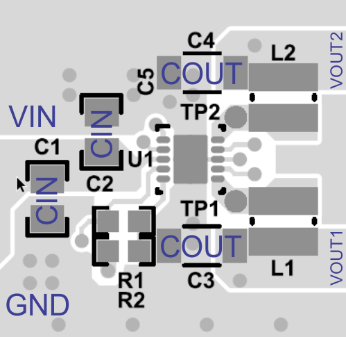
Layout Example

GUID-EC7D73AE-7CB3-44D1-BC78-8C6595FBFE3F-low.gifFigure 11-1 Layout Diagram