SLVS651B May 2006 – December 2015 TPS62510
PRODUCTION DATA.
- 1 Features
- 2 Applications
- 3 Description
- 4 Revision History
- 5 Pin Configuration and Functions
- 6 Specifications
- 7 Detailed Description
- 8 Application and Implementation
- 9 Power Supply Recommendations
- 10Layout
- 11Device and Documentation Support
- 12Mechanical, Packaging, and Orderable Information
Package Options
Mechanical Data (Package|Pins)
- DRC|10
Thermal pad, mechanical data (Package|Pins)
- DRC|10
Orderable Information
1 Features
- 1.8-V to 3.8-V Input Voltage Range
- Up to 96% High Efficiency Synchronous Step-Down Converter
- 1.5-MHz Fixed Frequency PWM Operation
- 1% Output Voltage Accuracy in Fixed Frequency PWM Mode
- Power Save Mode Operation for High Efficiency Over the Entire Load Current Range
- 22-μA Quiescent Current
- Adjustable Output Voltage
- Output Voltage Tracking (OVT) for Reliable Sequencing
- Available in a 3-mm × 3-mm 10-Pin VSON Package
2 Applications
- Portable Devices (Mobile Phone, Smartphone)
- 2-Cell NiMHd/Alkaline Applications
- Hard Disc Drives
- Point-of-Load Regulation
- Notebook Computers
- WiMAX and WLAN Applications
3 Description
The TPS62510 is a high-efficiency step-down converter targeted for operation from a 1.8-V to 3.8-V input voltage rail, ideally suited for 2-cell alkaline or NiMHd applications. The TPS62510 is also ideal as a point-of-load regulator running from a fixed 3.3-V, 2.5-V, or 1.8-V input voltage rail.
The converter operates in fixed frequency pulse width modulation (PWM) mode switching at 1.5 MHz with the MODE pin high. Pulling the MODE pin low enables the high efficiency mode. In high efficiency mode, the device operates with a 1.5-MHz fixed frequency PWM at nominal load current, and automatically enters the power save mode at light load currents. For maximum system reliability, the converter features output voltage tracking using the OVT pin to allow sequencing, and to allow for the output voltage to track an external voltage applied to this pin.
The TPS62510 is available in a 3-mm × 3-mm 10-pin VSON package.
Device Information(1)
| PART NUMBER | PACKAGE | BODY SIZE (NOM) |
|---|---|---|
| TPS62510 | VSON (10) | 3.00 mm × 3.00 mm |
- For all available packages, see the orderable addendum at the end of the data sheet.
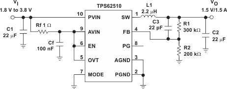
Typical Application Schematic

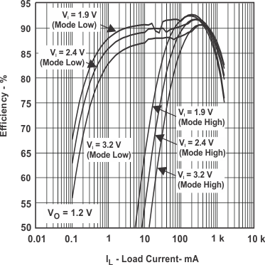
Efficiency vs Load Current
