SLVS651B May 2006 – December 2015 TPS62510
PRODUCTION DATA.
- 1 Features
- 2 Applications
- 3 Description
- 4 Revision History
- 5 Pin Configuration and Functions
- 6 Specifications
- 7 Detailed Description
- 8 Application and Implementation
- 9 Power Supply Recommendations
- 10Layout
- 11Device and Documentation Support
- 12Mechanical, Packaging, and Orderable Information
Package Options
Mechanical Data (Package|Pins)
- DRC|10
Thermal pad, mechanical data (Package|Pins)
- DRC|10
Orderable Information
8 Application and Implementation
NOTE
Information in the following applications sections is not part of the TI component specification, and TI does not warrant its accuracy or completeness. TI’s customers are responsible for determining suitability of components for their purposes. Customers should validate and test their design implementation to confirm system functionality.
8.1 Application Information
The TPS62510 is a high-efficiency step-down converter targeted for operation from a 1.8-V to 3.8-V input voltage rail, ideally suited for 2-cell alkaline or NiMHd applications. The TPS62510 is also ideal as a point-of-load regulator running from a fixed 3.3-V, 2.5-V or 1.8-V input voltage rail.
8.2 Typical Application
Figure 11 shows the adjustable version programming to 1.5 V.
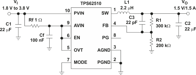 Figure 11. Adjustable Version Programmed to 1.5 V Example
8.2.1 Design Requirements
The design guideline provides a component selection to operate the device within the recommended operating conditions. The output voltage tracking is not used and the output voltage is programmed using the external voltage divider. The connection of the power good output is shown in one of the system examples.
8.2.2 Detailed Design Procedure
8.2.2.1 Input Capacitor Selection
Because of the nature of the buck converter having a pulsating input current, a low ESR input capacitor is required for best input voltage filtering, and minimizing the interference with other circuits caused by high input voltage spikes. The converter needs a ceramic input capacitor of 22 μF. The input capacitor may be increased without any limit for better input voltage filtering. The AVIN pin is separated from the power input of the converter. Note that the filter resistor may affect the undervoltage lockout threshold since up to 5 mA can flow via this resistor into the AVIN pin when the converter runs in PWM mode.
Table 1. Input Capacitor Selection
| CAPACITOR VALUE | CASE SIZE | COMPONENT SUPPLIER | COMMENTS |
|---|---|---|---|
| 22 μF | 1206 | TDK C3216X5R0J226M | Ceramic |
| 22 μF | 1206 | Taiyo Yuden JMK316BJ226ML | Ceramic |
8.2.2.2 Output Filter Design (Inductor and Output Capacitor)
The TPS62510 step-down converter has an internal loop compensation. Therefore, the external L-C filter must be selected to work with the internal compensation.
The internal compensation is optimized to operate with an output filter of L = 2.2 μH with an output capacitor of COUT = 22 μF. The output filter has its corner frequency per Equation 6:

where
- L = 2.2 μH
- CO = 22 μF
As a general rule of thumb, the product L x C should not move over a wide range when selecting a different output filter. This is because the internal compensation is designed to work with a certain output filter corner frequency, as calculated in Equation 6. This is especially important when selecting smaller inductor or output capacitor values that move the corner frequency to higher frequencies. However, when selecting the output filter a low limit for the inductor value exists due to other internal circuit limitations. The minimum inductor value for the TPS62510 should be kept at 2.2 μH. Selecting a larger capacitor value is less critical because the corner frequency drops, causing fewer stability issues.
Table 2. Output Capacitor Selection
| L | CO |
|---|---|
| 2.2 μH | ≥22 μF (ceramic capacitor) |
| 3.3 μH | ≥22 μF (ceramic capacitor)(1) |
8.2.2.3 Setting the Output Voltage Using the Feedback Resistor Divider
The external resistor divider sets the output voltage of the converter.
The output voltage is calculated as:

where
- R1 + R2 ≤ 1 MΩ
- The internal reference voltage is Vref typical = 0.6 V
To keep the operating quiescent current to a minimum, a high impedance feedback divider is selected with
R1 + R2 ≤ 1 MΩ. The sum of R1 and R2 should not be greater than 1 MΩ to avoid possible noise related regulation issues. A feedforward capacitor is needed across the upper feedback resistor to place a zero at a frequency of 25 kHz in the control loop. After selecting the feedback resistor values, the feedforward capacitor is calculated as:

where
- R1 = upper resistor of voltage divider
- Cff = upper capacitor of voltage divider
Select the capacitor value that is closest to the calculated value.
8.2.2.4 Inductor Selection
For high efficiencies, the inductor should have a low DC resistance to minimize conduction losses. Especially at high switching frequencies where the core material has a higher impact on the efficiency. The inductor value determines the inductor ripple current. The larger the inductor value, the smaller the inductor ripple current, and the lower the conduction losses of the converter. However, larger inductor values cause slower load transient response. Usually, the inductor ripple current as calculated in Equation 9, should be around 20% of the average output current.
To avoid saturation of the inductor, the inductor should be rated at least for the maximum output current of the converter plus the inductor ripple current calculated in Equation 9:

where
- f = Switching frequency (1.5 MHz typical)
- L = Inductor value
- ΔIL = Peak-to-peak inductor ripple current
- ILmax = Maximum inductor current
The highest inductor current occurs at maximum VIN.
A more conservative approach is to select the inductor current rating just for the maximum typical switch current limit of the converter of 2 A. See Table 3 for inductor recommendations.
Table 3. Inductor Recommendations
| INDUCTOR VALUE | COMPONENT SUPPLIER | DIMENSIONS | I(SAT) / R(DC) |
|---|---|---|---|
| 2.2 μH | Sumida CDRH2D18/HP 4R7 | 3.2 mm × 3.2 mm × 2 mm | 1.6 A / 60 mΩ |
| 2.2 μH | Wuerth 744045002 | 4.5 mm × 3.2 mm × 2.6 mm | 1.6 A / 110 mΩ |
| 2.2 μH | Sumida CDRH3D14 | 4 mm × 4 mm × 1.8 mm | 1.75 A / 69 mΩ |
| 2.2 μH | Sumida CDRH4D22 | 5 mm × 5 mm × 2.4 mm | 1.8 A / 25.4 mΩ |
| 2.2 μH | Sumida CDRH4D28 | 5 mm × 5 mm × 3 mm | 2 A / 31.3 mΩ |
| 2.2 μH | Coilcraft MSS5131 | 5.1 mm x 5.1 mm × 3.1 mm | 1.9 A / 23 mΩ |
| 2.2 μH | Coilcraft DO1608 | 6.6 mm × 4.45 mm × 2.92 mm | 2.3 A / 28 mΩ |
| 2.2 μH | Wuerth 74455022 | 6.6 mm × 4.45 mm × 2.92 mm | 2.3 A / 28 mΩ |
8.2.3 Application Curves
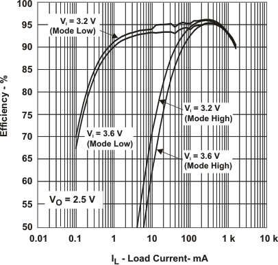 Figure 12. Efficiency vs Load Current, VOUT = 2.5 V
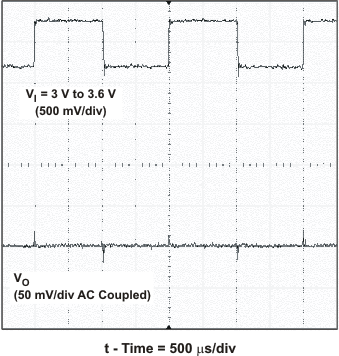 Figure 14. Line Transient Response
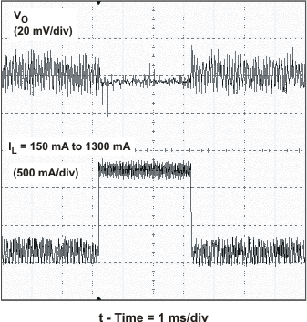 Figure 16. Load Transient, MODE = Low
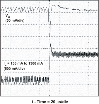 Figure 18. Rising Load Transient Response, MODE = Low
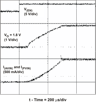 Figure 20. Soft Start-Up
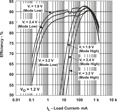 Figure 13. Efficiency vs Load Current, VOUT = 1.2 V
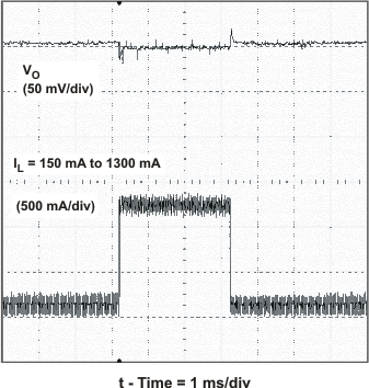 Figure 15. Load Transient Response, MODE = High
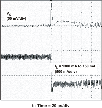 Figure 17. Falling Load Transient Response, MODE = Low
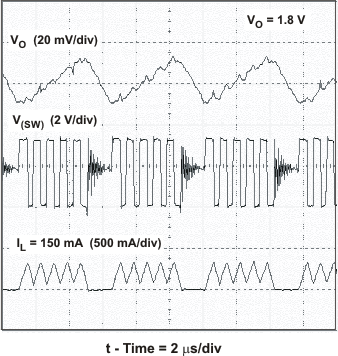 Figure 19. Power Save Mode Operation
8.3 System Example
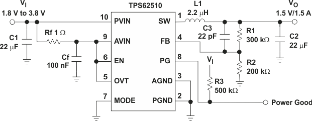 Figure 21. Adjustable Version Programmed to 1.5 V Using Power Good Example