SLVS897C January 2009 – December 2015 TPS62590
PRODUCTION DATA.
- 1 Features
- 2 Applications
- 3 Description
- 4 Revision History
- 5 Pin Configuration and Functions
- 6 Specifications
- 7 Detailed Description
- 8 Application and Implementation
- 9 Power Supply Recommendations
- 10Layout
- 11Device and Documentation Support
- 12Mechanical, Packaging, and Orderable Information
Package Options
Mechanical Data (Package|Pins)
- DRV|6
Thermal pad, mechanical data (Package|Pins)
- DRV|6
Orderable Information
7 Detailed Description
7.1 Overview
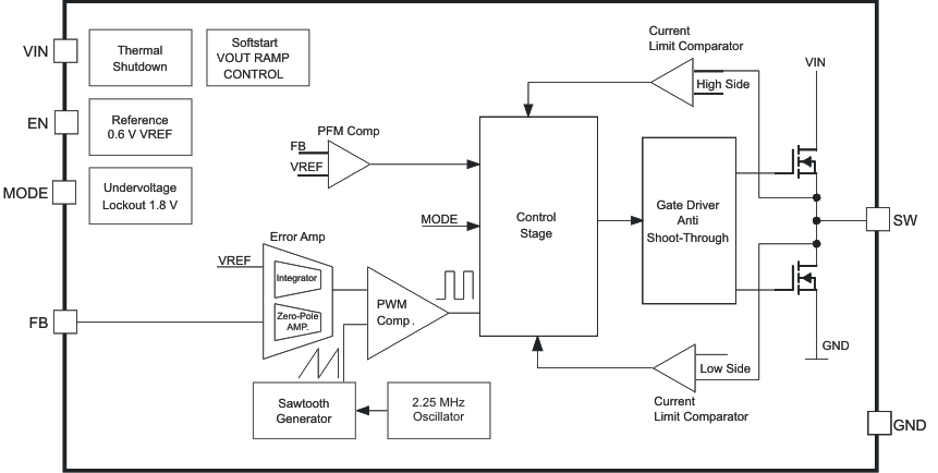
The TPS62590 step-down converter operates with typically 2.25-MHz fixed frequency pulse width modulation (PWM) at moderate to heavy load currents. At light load currents, the converter can automatically enter power save mode and operates then in pulse frequency modulation (PFM) mode.
During PWM operation, the converter use a unique fast response voltage mode controller scheme with input voltage feed-forward to achieve good line and load regulation allowing the use of small ceramic input and output capacitors. At the beginning of each clock cycle initiated by the clock signal, the high-side MOSFET switch is turned on. The current flows now from the input capacitor through the high-side MOSFET switch through the inductor to the output capacitor and load. During this phase, the current ramps up until the PWM comparator trips and the control logic turns off the switch. The current limit comparator also turns off the switch if the current limit of the high-side MOSFET switch is exceeded. After a dead time preventing shoot through current, the low-side MOSFET rectifier is turned on and the inductor current ramps down. The current flows now from the inductor to the output capacitor and to the load. It returns to the inductor through the low-side MOSFET rectifier.
The next cycle is initiated by the clock signal again turning off the low-side MOSFET rectifier and turning on the high-side MOSFET switch.
7.2 Functional Block Diagram

7.3 Feature Description
7.3.1 Dynamic Voltage Positioning
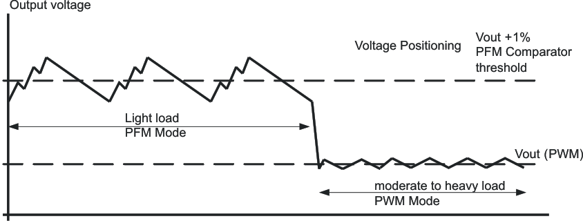
This feature reduces the voltage undershoots and overshoots at load steps from light to heavy load and vice versa. It is active in power-save mode and regulates the output voltage 1% higher than the nominal value. This provides more headroom for both the voltage drop at a load step, and the voltage increase at a load throw-off.
 Figure 5. Power-Save Mode Operation
7.3.2 Undervoltage Lockout
The undervoltage lockout circuit prevents the device from malfunctioning at low input voltages and from excessive discharge of the battery and disables the output stage of the converter. The undervoltage lockout threshold is typically 1.85 V with falling VIN.
7.3.3 Mode Selection
The MODE pin allows mode selection between forced PWM mode and power-save mode.
Connecting this pin to GND enables the power-save mode with automatic transition between PWM and PFM mode. Pulling the MODE pin high forces the converter to operate in fixed frequency PWM mode even at light load currents. This allows simple filtering of the switching frequency for noise-sensitive applications. In this mode, the efficiency is lower compared to the power-save mode during light loads.
The condition of the MODE pin can be changed during operation and allows efficient power management by adjusting the operation mode of the converter to the specific system requirements.
7.3.4 Enable
The device is enabled setting EN pin to high. During the start-up time tStart Up the internal circuits are settled. Afterwards, the device activates the soft-start circuit. The EN input can be used to control power sequencing in a system with various DC–DC converters. The EN pin can be connected to the output of another converter, to drive the EN pin high and getting a sequencing of supply rails. With EN = GND, the device enters shutdown mode. In this mode, all circuits are disabled. In fixed output voltage versions, the internal resistor divider network is disconnected from FB pin.
7.3.5 Thermal Shutdown
As soon as the junction temperature TJ exceeds 140°C (typical) the device goes into thermal shutdown. In this mode, the high-side and low-side MOSFETs are turned off. The device continues its operation when the junction temperature falls below the thermal shutdown hysteresis.
7.4 Device Functional Modes
7.4.1 Soft-Start
The TPS62590 has an internal soft-start circuit that controls the ramp up of the output voltage. The output voltage ramps up from 5% to 95% of its nominal value within typical 250 μs. This limits the inrush current in the converter during ramp up and prevents possible input voltage drops when a battery or high impedance power source is used. The soft start circuit is enabled within the start up time tStart Up.
7.4.2 Power-Save Mode
The power-save mode is enabled with MODE pin set to low level. If the load current decreases, the converter will enter power save mode operation automatically. During power save mode the converter skips switching and operates with reduced frequency in PFM mode with a minimum quiescent current to maintain high efficiency. The converter will position the output voltage +1% above the nominal output voltage typically. This voltage positioning feature minimizes voltage drops caused by a sudden load step.
The transition from PWM mode to PFM mode occurs once the inductor current in the low-side MOSFET switch becomes zero, which indicates discontinuous conduction mode.
During the power-save mode the output voltage is monitored with a PFM comparator. As the output voltage falls below the PFM comparator threshold of VOUT nominal +1%, the device starts a PFM current pulse. For this the high-side MOSFET switch will turn on and the inductor current ramps up. After the ON-time expires, the switch is turned off and the low-side MOSFET switch is turned on until the inductor current becomes zero.
The converter effectively delivers a current to the output capacitor and the load. If the load is below the delivered current, the output voltage will rise. If the output voltage is equal to or higher than the PFM comparator threshold, the device stops switching and enters a sleep mode with typical 15-μA current consumption.
If the output voltage is still below the PFM comparator threshold, a sequence of further PFM current pulses are generated until the PFM comparator threshold is reached. The converter starts switching again once the output voltage drops below the PFM comparator threshold.
With a fast single threshold comparator, the output voltage ripple during PFM mode operation can be kept small. The PFM pulse is time controlled, which allows to modify the charge transferred to the output capacitor by the value of the inductor. The resulting PFM output voltage ripple and PFM frequency depend in first order on the size of the output capacitor and the inductor value. Increasing output capacitor values and inductor values will minimize the output ripple. The PFM frequency decreases with smaller inductor values and increases with larger values.
The PFM mode is left and PWM mode entered in case the output current can not longer be supported in PFM mode. The power save mode can be disabled through the MODE pin set to high. The converter will then operate in fixed frequency PWM mode.
7.4.3 100% Duty Cycle Low Dropout Operation
The device starts to enter 100% duty cycle mode once the input voltage comes close the nominal output voltage. To maintain the output voltage, the high-side MOSFET switch is turned on 100% for one or more cycles.
With further decreasing VIN the high side MOSFET switch is turned on completely. In this case, the converter offers a low input-to-output voltage difference. This is particularly useful in battery-powered applications to achieve longest operation time by taking full advantage of the whole battery voltage range.
The minimum input voltage to maintain regulation depends on the load current and output voltage, and can be calculated by Equation 1:
where
- IOUTmax = Maximum output current plus inductor ripple current
- RDS(on)max = Maximum P-channel switch RDS(on)
- RL = DC resistance of the inductor
- VOUTmax = Nominal output voltage plus maximum output voltage tolerance
7.4.4 Short-Circuit Protection
The high-side and low side MOSFET switches are short-circuit protected with maximum switch current equal to ILIMF. The current in the switches is monitored by current limit comparators. Once the current in the high-side MOSFET switch exceeds the threshold of its current limit comparator, it turns off and the low-side MOSFET switch is activated to ramp down the current in the inductor and high-side MOSFET switch. The high-side MOSFET switch can only turn on again, once the current in the low-side MOSFET switch has decreased below the threshold of its current limit comparator.