SLVS952G April 2010 – January 2017 TPS62671 , TPS62672 , TPS62674 , TPS62675 , TPS626751 , TPS626765 , TPS62679
PRODUCTION DATA.
- 1 Features
- 2 Applications
- 3 Description
- 4 Simplified Schematic
- 5 Revision History
- 6 Device Comparison Table
- 7 Pin Configuration and Functions
- 8 Specifications
- 9 Parameter Measurement Information
- 10Detailed Description
- 11Application and Implementation
- 12Power Supply Recommendations
- 13Layout
- 14Device and Documentation Support
- 15Mechanical, Packaging, and Orderable Information
Package Options
Mechanical Data (Package|Pins)
- YFD|6
Thermal pad, mechanical data (Package|Pins)
Orderable Information
13 Layout
13.1 Layout Guidelines
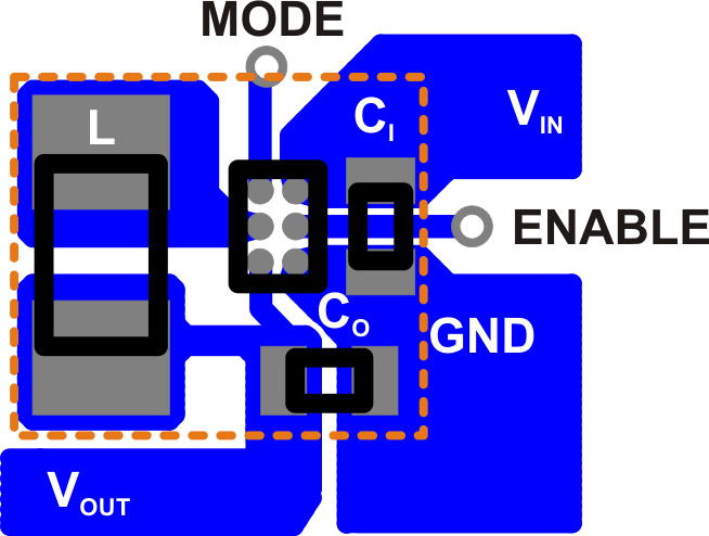
As for all switching power supplies, the layout is an important step in the design. High-speed operation of the TPS6267x devices demand careful attention to PCB layout. Care must be taken in board layout to get the specified performance. If the layout is not carefully done, the regulator could show poor line and/or load regulation, stability and switching frequency issues as well as EMI problems. It is critical to provide a low inductance, impedance ground path. Therefore, use wide and short traces for the main current paths.
The ground pins of the dc/dc converter must be strongly connected to the PCB ground (i.e. reference potential across the system). These ground pins serve as the return path for both the control circuitry and the synchronous rectifier. Furthermore, due to its high frequency switching circuitry, it is imperative for the input capacitor to be as close to the SMPS device as possible, and that there is an unbroken ground plane under the TPS6267x and its external passives. Additionally, minimizing the area between the SW pin trace and inductor will limit high frequency radiated energy. The feed-back line should be routed away from noisy components and traces (e.g. SW line).
The output capacitor carries the inductor ripple current. While not as critical as the input capacitor, an unbroken ground connection from this capacitor’s ground return to the inductor, input capacitor and SMPS device will reduce the output voltage ripple and it’s associated ESL step. This is a critical aspect to achieve best loop and frequency stability.
High frequency currents tend to find their way on the ground plane along a mirror path directly beneath the incident path on the top of the board. If there are slits or cuts in the ground plane due to other traces on that layer, the current will be forced to go around the slits. If high frequency currents are not allowed to flow back through their natural least-area path, excessive voltage will build up and radiated emissions will occur. There should be a group of vias in the surrounding of the dc/dc converter leading directly down to an internal ground plane. To minimize parasitic inductance, the ground plane should be as close as possible to the top plane of the PCB (i.e. onto which the components are located).
13.2 Layout Example
 Figure 53. Suggested Layout (Top)