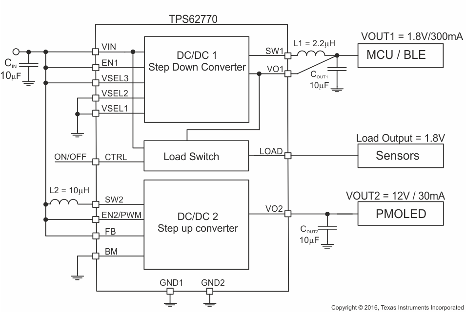
The TPS62770 is a tiny power solution for wearable applications including a 370nA ultra low Iq step-down converter, a slew rate controlled load switch and a dual mode step-up converter. The output voltage of the step-down converter can be selected with three VSEL pins between 1.0 V, 1.05 V, 1.1 V, 1.2 V, 1.8 V, 1.9 V, 2.0 V and 3.0 V. The output voltage can be changed during operation. In shutdown mode, the output of the step-down converter is pulled to GND. The integrated load switch is internally connected to the output of the step-down converter and features slew rate control during turn on phase. Once turned off, its output is connected to GND.
The dual mode step-up converter can generate a constant output voltage up to 15 V, such as PMOLED supply; or, a constant output current, such as LED back light supply. The output voltage can be adjusted up to 15 V with external resistors, or set to fixed 12 V by connecting the FB pin to VIN. The device features an internal over voltage protection of 17.7 V in case the FB node is left open or tight to GND. It includes an internal rectifier and load disconnect function. When used as constant output current driver, the device offers a PWM to analog converter to scale down the reference voltage according to the duty cycle of the PWM signal.
The device is available in a small 16pin 0.4mm pitch WCSP package.
PART NUMBER | PACKAGE | BODY SIZE (NOM) |
---|---|---|
TPS62770 | DSBGA (16) | 1.58mm x 1.58mm |
PIN | I/O | DESCRIPTION | |
---|---|---|---|
NAME | NO | ||
EN2/PWM | B3 | IN | Enable pin for the step-up converter. High level enables the devices, low level turns the device into shutdown mode. A PWM signal can be applied to this pin when used as a constant current driver (BM pin connected to VIN). The pin must be terminated. |
GND2 | A1 | PWR | GND supply pin for the step-up converter. Connect this pin close to the GND terminals of the input and output capacitors. |
SW2 | A2 | IN | The switch pin of the step-up converter. It is connected to the drain of the internal power MOSFET. Connect the inductor L2 between this pin and the input capacitor CIN |
VO2 | A3 | OUT | Output of the step-up converter. |
BM | B1 | IN | This pin controls the operation mode of the step-up converter. With BM = high, the device features a low feedback voltage of 200mV, which can be scaled down by the integrated PWM to analog converter. With BM = low, the device operates with a 0.8V feedback voltage and operates as a step-up converter with voltage regulation. This pin must be terminated and set before the device is enabled. |
FB | B4 | IN | Feedback pin for the step-up converter to set the output voltage / current. Connect the pin to the center tap of a resistor divider to program the output voltage. When it is connected to the VIN pin, the output voltage is set to 12 V by an internal feedback divider network. When used as a LED current driver connect the sense resistor between this pin and GND. The LED string is connected between FB pin and VO2. |
EN1 | C2 | IN | Enable pin for the step-down converter. High level enables the devices, low level turns the device into shutdown mode. The pin must be terminated. |
VSEL1 | C3 | IN | Output voltage selection pins. See Output Voltage Setting Step-Down Converter for VOUT selection. These pins must be terminated. The pins can be dynamically changed during operation. |
VSEL2 | B2 | IN | |
VSEL3 | A4 | IN | |
CTRL | C4 | IN | This pin controls the load switch between VO1 and LOAD. With CTRL = low, the LOAD switch is disabled. The pin must be terminated. |
VIN | D1 | PWR | VIN power supply pin. Connect the input capacitor close to this pin for best noise and voltage spike suppression. A ceramic capacitor of 10μF is required. |
GND1 | D2 | PWR | GND supply pin for the step-down converter. Connect this pin close to both, the GND terminal of the input and output capacitor. |
SW1 | C1 | OUT | This is the switch pin of the step-down converter and is connected to the internal MOSFET switches. Connect the inductor L1 between this terminal and the output capacitor. |
VO1 | D3 | OUT | Output of the step-down converter. The output voltage is sensed via this pin to the internal feedback divider network for the regulation loop. In addition the internal load switch is connected between VO1 pin and LOAD pin. Connect this pin directly to the output capacitor with a short trace. The pin is connected to GND1 and discharges the output capacitor when the converter is disabled. |
LOAD | D4 | OUT | Output terminal of the internal load switch. With CTRL = high, the internal load switch connects VO1 to the LOAD pin. The switch features a slew rate control. This pin is pulled to GND with the CTRL = low. If not used, leave the pin open. |
VO1 [V] | VSEL3 | VSEL2 | VSEL1 |
---|---|---|---|
1.0 | 0 | 0 | 0 |
1.05 | 0 | 0 | 1 |
1.1 | 0 | 1 | 0 |
1.2 | 0 | 1 | 1 |
1.8 | 1 | 0 | 0 |
1.9 | 1 | 0 | 1 |
2.0 | 1 | 1 | 0 |
3.0 | 1 | 1 | 1 |
MIN | MAX | UNIT | |||
---|---|---|---|---|---|
Pin voltage(2) | VIN, FB | –0.3 | 6 | V | |
SW1 | –0.3 | VIN +0.3V | V | ||
EN1, EN2/PWM, CTRL, BM, VSEL1-3 | –0.3 | VIN +0.3V | V | ||
SW2, VO2 | -0.3 | 32 | V | ||
VO1, LOAD | –0.3 | 3.7 | V | ||
TJ | Operating junction temperature range | –40 | 125 | °C | |
Tstg | Storage temperature range | –65 | 150 | °C |
VALUE | UNIT | ||||
---|---|---|---|---|---|
V(ESD) | Electrostatic discharge | Human body model (HBM), per ANSI/ESDA/JEDEC JS-001, all pins(1) | ± 2000 | V | |
Charged device model (CDM), per JEDEC specification JESD22-C101, all pins(2) | ±500 |
MIN | NOM | MAX | UNIT | ||||||
---|---|---|---|---|---|---|---|---|---|
VIN | Input voltage range at VIN pin | 2.5 | 5.5 | V | |||||
IOUT1 | DC/DC 1 Step down converter output current | L1 = 2.2µH, COUT1 = 10 µF | 300 | mA | |||||
IOUT2 | DC/DC 2 Step up converter output current | 2.5V < VIN < 5.5V, VOUT2 = 12V, COUT2 = 10uF, L = 10µH | 30 | mA | |||||
2.5V < VIN < 5.5V, VOUT2 = 12V, COUT2 = 2x 10uF, L = 10µH | 100 | ||||||||
3V < VIN < 5.5V, VOUT2 = 5V, COUT2 = 2x 10uF, L = 4.7µH | 200 | ||||||||
ILOAD | Load current (current from LOAD pin) | 100 | |||||||
TJ | Operating junction temperature range | -40 | 125 | °C | |||||
TA | Ambient temperature range | -40 | 85 |
THERMAL METRIC(1) | TPS62770 | UNIT | |
---|---|---|---|
YFP | |||
TERMINALS | |||
RθJA | Junction-to-ambient thermal resistance | 90.6 | °C/W |
RθJCtop | Junction-to-case (top) thermal resistance | 0.6 | |
RθJB | Junction-to-board thermal resistance | 13.8 | |
ψJT | Junction-to-top characterization parameter | 2.8 | |
ψJB | Junction-to-board characterization parameter | 13.7 | |
RθJCbot | Junction-to-case (bottom) thermal resistance | n/a |
PARAMETER | TEST CONDITIONS | MIN | TYP | MAX | UNIT | |||
---|---|---|---|---|---|---|---|---|
SUPPLY | ||||||||
ISD | Shutdown current into VIN | EN1 = EN2/PWM = GND, CTRL GND, BM = GND, | 0.1 | 1850 | nA | |||
VTH_ UVLO+ | Undervoltage lockout threshold | Rising VIN | 2.1 | 2.22 | V | |||
VTH_UVLO- | Falling VIN | 1.9 | 2 | |||||
INPUTS EN1, EN2/PWM, BM, CTRL,VSEL 1-3 | ||||||||
VIH TH | High level input threshold | 1.2 | V | |||||
VIL TH | Low level input threshold | 0.4 | V | |||||
IIN | Input bias Current | TJ = 25°C | 10 | nA | ||||
TJ = –40°C to 85°C | 25 | |||||||
STEP-DOWN CONVERTER | ||||||||
IQ | Operating quiescent current | EN1 = VIN, EN2/PWM = GND, CTRL = GND, IOUT = 0µA, VOUT = 1.8V, device not switching, | 370 | 1850 | nA | |||
EN1 = VIN, EN2/PWM = GND, IOUT = 0mA, CTRL = GND, VOUT = 1.8V , device switching | 500 | |||||||
VVOUT | Output voltage range | 1.0 | 3.0 | V | ||||
Output voltage accuracy | PFM mode | -2.5 | 0 | 2.5 | % | |||
PWM mode | -2 | 0 | 2 | |||||
DC output voltage load regulation | VOUT = 1.8V | 0.001 | %/mA | |||||
DC output voltage line regulation | VOUT = 1.8V, IOUT = 10 mA, 2.5V ≤ VIN ≤ 5.5V | 0 | %/V | |||||
RDS(ON) | High side MOSFET on-resistance | IOUT = 50mA | 0.45 | Ω | ||||
Low Side MOSFET on-resistance | 0.22 | |||||||
ILIMF | High side MOSFET switch current limit | 480 | 600 | 720 | mA | |||
Low side MOSFET switch current limit | 600 | mA | ||||||
RDSCH_VO1 | Discharge switch on-resistance | EN = GND, IVO1 = -10mA into VO1 pin | 20 | 65 | Ω | |||
IIN_VO1 | Bias current into VO1 pin | EN = VIN, VOUT = 1.8V | TJ = 25°C | 40 | 100 | nA | ||
TJ = –40°C to 85°C | 1010 | |||||||
VTH_100+ | Auto 100% Mode leave detection threshold (1) | Rising VIN,100% Mode is left with VIN = VOUT + VTH_100+ , max value at TJ = 85°C | 150 | 250 | 370 | mV | ||
VTH_100- | Auto 100% Mode enter detection threshold (1) | Falling VIN, 100% Mode is entered with VIN = VOUT + VTH_100-, max value at TJ = 85°C | 85 | 200 | 310 | |||
tONmin | Minimum ON time | VOUT = 2.0V, IOUT = 0 mA | 225 | ns | ||||
tOFFmin | Minimum OFF time | 50 | ns | |||||
tStartup_delay | Regulator start up delay time | From transition EN1 = low to high until device starts switching | 1 | 5 | ms | |||
tSoftstart | Softstart time with reduced switch current limit | 700 | 1200 | µs | ||||
ILIM_softstart | High side MOSFET switch current limit | Reduced switch current limit during softstart | 80 | 150 | 200 | mA | ||
Low side MOSFET switch current limit | 150 | |||||||
LOAD SWITCH | ||||||||
RLOAD | MOSFET on-resistance | ILOAD = 50mA, CTRL = VIN, VOUT = 1.8V, | 0.6 | 1.27 | Ω | |||
trise_LOAD | VLOAD rise time | Starting with CTRL low to high transition, time to ramp VLOAD from 95%, VOUT = 1.8V, ILOAD = 20mA | 315 | 800 | μs | |||
RDCHRG | MOSFET on-resistance | 20 | 65 | Ω | ||||
STEP-UP CONVERTER | ||||||||
IQ_VIN | Quiescent current into VIN pin | EN2/PWM = VIN, BM = GND, EN1 = GND, no load, no switching, VOUT = 12 V | 110 | 200 | µA | |||
VOUT | Output voltage range | EN2/PWM = VIN, BM = GND | 4.5 | 15 | V | |||
VOUT_12V | 12-V output voltage accuracy | FB pin connected to VIN pin, EN2/PWM = VIN, BM = GND | 11.7 | 12 | 12.3 | V | ||
VFB | Feedback voltage | PWM mode, BM = GND, EN2/PWM = VIN | 0.775 | 0.795 | 0.814 | V | ||
PFM mode, BM = GND, EN2/PWM = VIN | 0.803 | V | ||||||
Feedback regulation voltage under brightness control | EN2/PWM = VIN, BM = VIN, | 189 | 200 | 206 | mV | |||
VFB =50mV, BM = VIN, D(PWM) @ EN2/PWM = 25%, | 40 | 50 | 60 | mV | ||||
VFB = 20mV, BM = VIN, D(PWM) @ EN2/PWM = 10% | 13 | 20 | 27 | |||||
tDim_Off | Dimming signal on pin EN2/PWM | 270 | 160 | μs | ||||
tDim_On | 1 | μs | ||||||
VOVP | Output overvoltage protection threshold | 17 | 17.7 | 18.4 | V | |||
VOVP_HYS | Over voltage protection hysteresis | 800 | mV | |||||
IFB_LKG | Leakage current into FB pin | 5 | 200 | nA | ||||
ISW_LKG | Leakage current into SW pin | EN2/PWM = GND | 5 | 500 | nA | |||
RDS(on) | Isolation MOSFET on resistance | VOUT = 12 V | 850 | mΩ | ||||
Low-side MOSFET on resistance | VOUT = 12 V | 450 | ||||||
fSW | Switching frequency | VOUT = 12 V, PWM mode | 850 | 1050 | 1250 | kHz | ||
tON_min | Minimal switch on time | 150 | 250 | ns | ||||
ILIM_SW | Peak switch current limit | VOUT = 12 V | 730 | 970 | 1230 | mA | ||
ILIM_CHG | Pre-charge current | VOUT = 0 V | 30 | 55 | mA | |||
tSoftstart | Pre-charge time | BM = GND, EN2/PWM from low to high until device starts switching, IOUT2 = 0mA, COUT2 = 10uF | 6 | ms | ||||
Startup time | VOUT from VIN to 12 V, COUT_effective = 2.2 µF, IOUT = 0 A | 6 |
EN2/PWM = Low | VOUT1 Set to 1.8 V | |
EN1 = High | Device not Switching | |
EN1 = EN2/PWM = Low | ||
EN2/PWM = High | VOUT2 Set to 12 V | |
EN1 = Low | Device not Switching | |