SLVSDD1G December   2017  – June 2024 TPS62800 , TPS62801 , TPS62802 , TPS62806 , TPS62807 , TPS62808

PRODUCTION DATA  

  1.   1
  2. Features
  3. Applications
  4. Description
  5. Device Comparison Table
  6. Pin Configuration and Functions
  7. Specifications
    1. 6.1 Absolute Maximum Ratings
    2. 6.2 ESD Ratings
    3. 6.3 Recommended Operating Conditions
    4. 6.4 Thermal Information
    5. 6.5 Electrical Characteristics
    6. 6.6 Typical Characteristics
  8. Detailed Description
    1. 7.1 Overview
    2. 7.2 Functional Block Diagram
    3. 7.3 Feature Description
      1. 7.3.1 Smart Enable and Shutdown (EN)
      2. 7.3.2 Soft Start
      3. 7.3.3 VSEL/MODE Pin
        1. 7.3.3.1 Output Voltage Selection (R2D Converter)
        2. 7.3.3.2 Mode Selection — Power Save Mode and Forced PWM Operation
      4. 7.3.4 Undervoltage Lockout (UVLO)
      5. 7.3.5 Switch Current Limit and Short Circuit Protection
      6. 7.3.6 Thermal Shutdown
      7. 7.3.7 Output Voltage Discharge
    4. 7.4 Device Functional Modes
      1. 7.4.1 Power Save Mode Operation
      2. 7.4.2 Forced PWM Mode Operation
      3. 7.4.3 100% Mode Operation
      4. 7.4.4 Optimized Transient Performance from PWM-to-PFM Mode Operation
  9. Application and Implementation
    1. 8.1 Application Information
    2. 8.2 Typical Application
      1. 8.2.1 Design Requirements
      2. 8.2.2 Detailed Design Procedure
        1. 8.2.2.1 Custom Design With WEBENCH® Tools
        2. 8.2.2.2 Inductor Selection
        3. 8.2.2.3 Output Capacitor Selection
        4. 8.2.2.4 Input Capacitor Selection
      3. 8.2.3 Application Curves
    3. 8.3 System Examples
    4. 8.4 Power Supply Recommendations
    5. 8.5 Layout
      1. 8.5.1 Layout Guidelines
      2. 8.5.2 Layout Example
  10. Device and Documentation Support
    1. 9.1 Device Support
      1. 9.1.1 Third-Party Products Disclaimer
      2. 9.1.2 Development Support
        1. 9.1.2.1 Custom Design With WEBENCH® Tools
    2. 9.2 Receiving Notification of Documentation Updates
    3. 9.3 Support Resources
    4. 9.4 Trademarks
    5. 9.5 Electrostatic Discharge Caution
    6. 9.6 Glossary
  11. 10Revision History
  12. 11Mechanical, Packaging, and Orderable Information
    1. 11.1 Mechanical Data

Package Options

Refer to the PDF data sheet for device specific package drawings

Mechanical Data (Package|Pins)
  • YKA|6
Thermal pad, mechanical data (Package|Pins)
Orderable Information

Optimized Transient Performance from PWM-to-PFM Mode Operation

For most converters, the load transient response in PWM mode is improved compared to PFM mode, because the converter reacts faster on the load step and actively sinks energy on the load release. Compare Figure 8-33 to Figure 8-32. As an additional feature, the TPS6280x automatically enters PWM mode for 16 cycles after a heavy load release to bring the output voltage back to the regulation level faster. After 16 cycles of PWM mode, the device automatically returns to PFM mode (if VSEL/MODE is driven low). See Figure 7-2. Without this optimization, the output voltage overshoot would be higher and would look like the VOUT' trace. This feature is only active after the load is high enough and the converter operates in PWM mode.
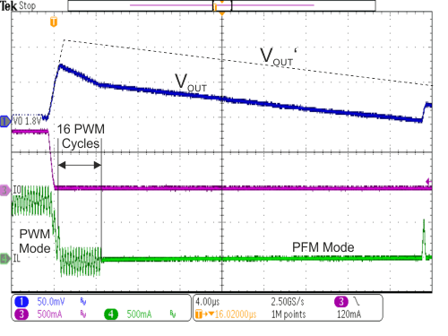
TPS62800 TPS62801 TPS62802 TPS62806 TPS62807 TPS62808 Optimized Transient
                        Performance from PWM-to-PFM ModeFigure 7-2 Optimized Transient Performance from PWM-to-PFM Mode