SLVSDD1G December 2017 – June 2024 TPS62800 , TPS62801 , TPS62802 , TPS62806 , TPS62807 , TPS62808
PRODUCTION DATA
- 1
- 1 Features
- 2 Applications
- 3 Description
- 4 Device Comparison Table
- 5 Pin Configuration and Functions
- 6 Specifications
-
7 Detailed Description
- 7.1 Overview
- 7.2 Functional Block Diagram
- 7.3 Feature Description
- 7.4 Device Functional Modes
- 8 Application and Implementation
- 9 Device and Documentation Support
- 10Revision History
- 11Mechanical, Packaging, and Orderable Information
Package Options
Refer to the PDF data sheet for device specific package drawings
Mechanical Data (Package|Pins)
- YKA|6
Thermal pad, mechanical data (Package|Pins)
Orderable Information
3 Description
The TPS6280x device family is a step-down converter with 2.3µA typical quiescent current featuring the highest efficiency and smallest design size. TI's DCS-Control topology enables the device to operate with tiny inductors and capacitors with a switching frequency up to 4MHz. At light load conditions, the device seamlessly enters power save mode to reduce switching cycles and maintain high efficiency.
Connecting the VSEL/MODE pin to GND selects a fixed output voltage. With only one external resistor connected to VSEL/MODE pin, 16 internally set output voltages can be selected. An integrated R2D (resistor-to-digital) converter reads out the external resistor and sets the output voltage. The same device part number can be used for different applications and voltage rails just by changing a single resistor. Furthermore, the internally set output voltage provides better accuracy compared to a traditional external resistor divider network. After the device has started up, the DC/DC converter enters forced PWM mode by applying a high level at the VSEL/MODE pin. In this operating mode, the device runs at a typical 4MHz or 1.5MHz switching frequency, enabling lowest output voltage ripple and highest efficiency. The TPS6280x device series comes in a tiny 6-pin WCSP package with 0.35mm pitch.
| PART NUMBER(3) | PACKAGE(1) | PACKAGE SIZE(2) |
|---|---|---|
| TPS62800 | YKA (DSBGA, 6) | 1.05 mm × 0.70 mm |
| TPS62801 | ||
| TPS62802 | ||
| TPS62806 | ||
| TPS62807 |
 Typical Application
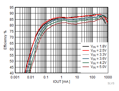
 Efficiency Versus
IOUT at 1.2VOUT