SLUSDM1A March   2020  – December 2021 TPS62816-Q1

PRODUCTION DATA  

  1. Features
  2. Applications
  3. Description
  4. Revision History
  5. Device Comparison Table
  6. Pin Configuration and Functions
  7. Specifications
    1. 7.1 Absolute Maximum Ratings
    2. 7.2 ESD Ratings
    3. 7.3 Recommended Operating Conditions
    4. 7.4 Thermal Information
    5. 7.5 Electrical Characteristics
    6. 7.6 Typical Characteristics
  8. Parameter Measurement Information
  9. Detailed Description
    1. 9.1 Overview
    2. 9.2 Functional Block Diagram
    3. 9.3 Feature Description
      1. 9.3.1 Precise Enable
      2. 9.3.2 COMP/FSET
      3. 9.3.3 MODE/SYNC
      4. 9.3.4 Spread Spectrum Clocking (SSC)
      5. 9.3.5 Undervoltage Lockout (UVLO)
      6. 9.3.6 Power Good Output (PG)
      7. 9.3.7 Thermal Shutdown
    4. 9.4 Device Functional Modes
      1. 9.4.1 Pulse Width Modulation (PWM) Operation
      2. 9.4.2 Power Save Mode Operation (PWM/PFM)
      3. 9.4.3 100% Duty-Cycle Operation
      4. 9.4.4 Current Limit and Short Circuit Protection
      5. 9.4.5 Foldback Current Limit and Short Circuit Protection
      6. 9.4.6 Output Discharge
      7. 9.4.7 Soft Start/Tracking (SS/TR)
  10. 10Application and Implementation
    1. 10.1 Application Information
      1. 10.1.1 Programming the Output Voltage
      2. 10.1.2 External Component Selection
        1. 10.1.2.1 Inductor Selection
        2. 10.1.2.2 Capacitor Selection
          1. 10.1.2.2.1 Input Capacitor
          2. 10.1.2.2.2 Output Capacitor
    2. 10.2 Typical Application
      1. 10.2.1 Design Requirements
      2. 10.2.2 Detailed Design Procedure
      3. 10.2.3 Application Curves
    3. 10.3 System Examples
      1. 10.3.1 Voltage Tracking
      2. 10.3.2 Synchronizing to an External Clock
      3. 10.3.3 Compensation Settings
  11. 11Power Supply Recommendations
  12. 12Layout
    1. 12.1 Layout Guidelines
    2. 12.2 Layout Example
  13. 13Device and Documentation Support
    1. 13.1 Device Support
      1. 13.1.1 Third-Party Products Disclaimer
    2. 13.2 Documentation Support
      1. 13.2.1 Related Documentation
    3. 13.3 Receiving Notification of Documentation Updates
    4. 13.4 Support Resources
    5. 13.5 Trademarks
    6. 13.6 Electrostatic Discharge Caution
    7. 13.7 Glossary
  14. 14Mechanical, Packaging, and Orderable Information

Package Options

Mechanical Data (Package|Pins)
Thermal pad, mechanical data (Package|Pins)
Orderable Information

Parameter Measurement Information

The graphs in this data sheet have been taken based on the schematic and BOM as listed in Table 8-1 if not otherwise mentioned in the plots.
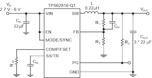
GUID-3EC61906-3D51-4BF1-88F2-37A02C87AD9A-low.gif Figure 8-1 Measurement Setup for TPS62816-Q1
Table 8-1 List of Components
REFERENCE DESCRIPTION MANUFACTURER (1)
IC TPS62816-Q1 Texas Instruments
L 0.25-µH inductor; XGL4020-251ME Coilcraft
CIN 22 µF / 10 V; GCM31CR71A226KE02L Murata
COUT for VOUT = 0.6 V 5 × 22 µF / 10 V; GCM31CR71A226KE02L Murata
COUT for VOUT ≥ 1 V 3 × 22 µF / 10 V; GCM31CR71A226KE02L Murata
CSS 15 nF (equal to 0.9-ms start-up ramp) any
RCF 8.06 kΩ any
CFF 10 pF any
R1 Depending on VOUT any
R2 Depending on VOUT any
R3 100 kΩ any