SLVSEF9I March 2018 – March 2024 TPS62824 , TPS62824A , TPS62825 , TPS62825A , TPS62826 , TPS62826A , TPS62827 , TPS62827A
PRODUCTION DATA
- 1
- 1 Features
- 2 Applications
- 3 Description
- 4 Device Options
- 5 Pin Configuration and Functions
- 6 Specifications
- 7 Detailed Description
- 8 Application and Implementation
- 9 Device and Documentation Support
- 10Revision History
- 11Mechanical, Packaging, and Orderable Information
Package Options
Mechanical Data (Package|Pins)
- DMQ|6
Thermal pad, mechanical data (Package|Pins)
Orderable Information
3 Description
The TPS6282x is an easy-to-use, synchronous step-down DC/DC converters family with a very low quiescent current of only 4μA. Based on the DCS-Control topology, the device provides a fast transient response. The internal reference allows to regulate the output voltage down to 0.6V with a high feedback voltage accuracy of 1% over the junction temperature range of –40°C to 125°C. The family devices are pin-to-pin and BOM-to-BOM compatible. The entire design requires a small 470nH inductor, a single 4.7µF input capacitor, and two 10µF or single 22µF output capacitor.
The TPS6282x is available in two flavors. The first includes an automatically entered power save mode to maintain high efficiency down to very light loads for extending the system battery run-time. The second runs in forced-PWM maintaining a continuous conduction mode to make sure of the least ripple in the output voltage and a quasi-fixed switching frequency. The device features a Power-Good signal and an internal soft-start circuit. The device is able to operate in 100% mode. For fault protection, the device incorporates a HICCUP short-circuit protection as well as a thermal shutdown. The device is available in a 6-pin 1.5mm × 1.5mm QFN package, offering the highest power density design.
 Typical Application
Schematic
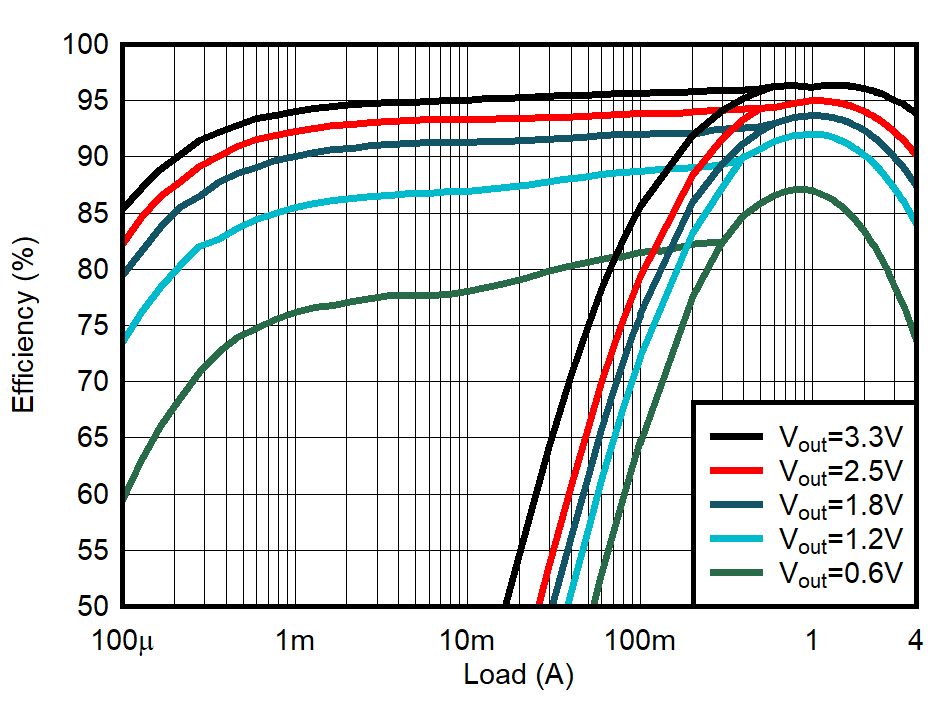
 Efficiency at VIN = 5V