SLVSG98B February   2023  – March 2024 TPS628301 , TPS628302 , TPS628303 , TPS628304

PRODUCTION DATA  

  1.   1
  2. Features
  3. Applications
  4. Description
  5. Device Options
  6. Pin Configuration and Functions
  7. Specifications
    1. 6.1 Absolute Maximum Ratings
    2. 6.2 ESD Ratings
    3. 6.3 Recommended Operating Conditions
    4. 6.4 Thermal Information Discrete
    5. 6.5 Electrical Characteristics
    6. 6.6 Typical Characteristics
  8. Detailed Description
    1. 7.1 Overview
    2. 7.2 Functional Block Diagram
    3. 7.3 Feature Description
      1. 7.3.1 Pulse Width Modulation (PWM) Operation
      2. 7.3.2 Power Save Mode (PSM) Operation
      3. 7.3.3 Start-Up and Soft Start
      4. 7.3.4 Switch Cycle-by-Cycle Current Limit
      5. 7.3.5 Short-Circuit Protection
      6. 7.3.6 Undervoltage Lockout
      7. 7.3.7 Thermal Shutdown
      8. 7.3.8 Optimized EMI Performance
    4. 7.4 Device Functional Modes
      1. 7.4.1 Enable, Disable, and Output Discharge
      2. 7.4.2 Minimum Duty Cycle and 100% Mode Operation
      3. 7.4.3 Power Good
  9. Application and Implementation
    1. 8.1 Application Information
    2. 8.2 Typical Application
      1. 8.2.1 Design Requirements
      2. 8.2.2 Detailed Design Procedure
        1. 8.2.2.1 Custom Design With WEBENCH® Tools
        2. 8.2.2.2 Setting The Output Voltage
        3. 8.2.2.3 Inductor Selection
        4. 8.2.2.4 Output Capacitor Selection
        5. 8.2.2.5 Input Capacitor Selection
      3. 8.2.3 Application Curves
    3. 8.3 Power Supply Recommendations
    4. 8.4 Layout
      1. 8.4.1 Layout Guidelines
      2. 8.4.2 Layout Example
        1. 8.4.2.1 Thermal Considerations
  10. Device and Documentation Support
    1. 9.1 Device Support
      1. 9.1.1 Third-Party Products Disclaimer
      2. 9.1.2 Development Support
        1. 9.1.2.1 Custom Design With WEBENCH® Tools
    2. 9.2 Documentation Support
      1. 9.2.1 Related Documentation
    3. 9.3 Support Resources
    4. 9.4 Trademarks
    5. 9.5 Electrostatic Discharge Caution
    6. 9.6 Glossary
  11. 10Revision History
  12. 11Mechanical, Packaging, and Orderable Information

Package Options

Mechanical Data (Package|Pins)
Thermal pad, mechanical data (Package|Pins)
Orderable Information

Application Curves

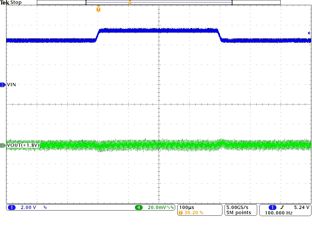
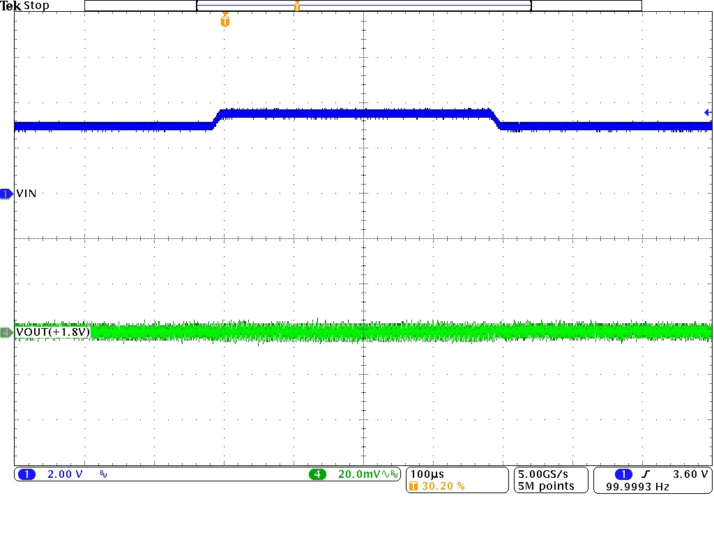
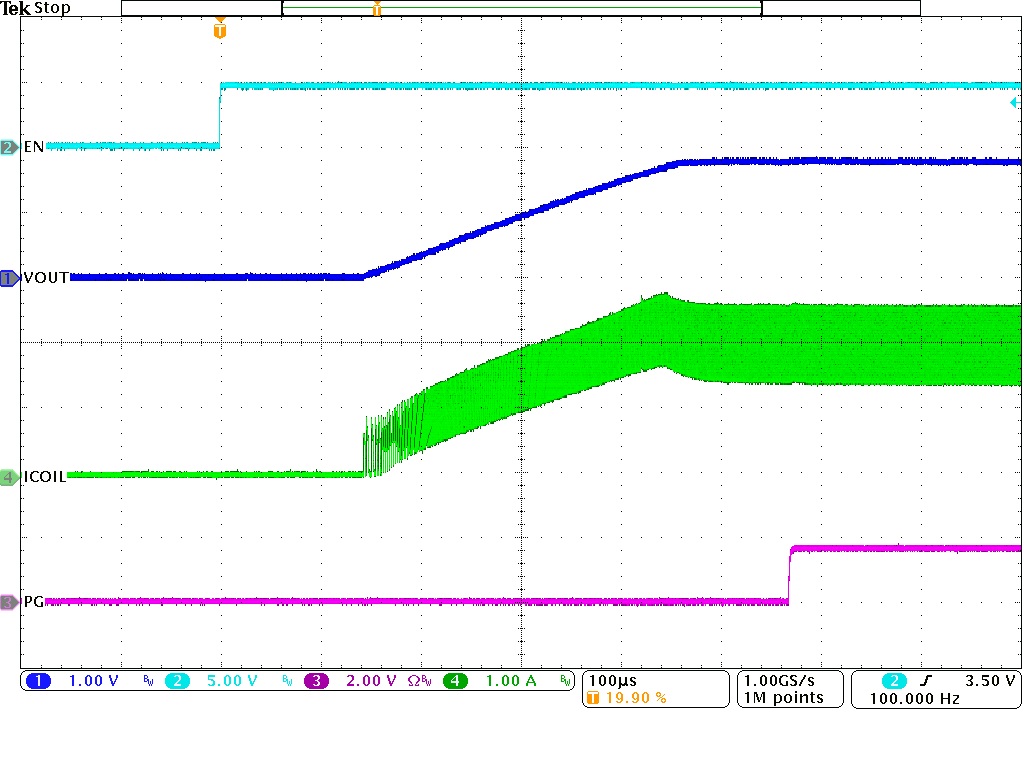
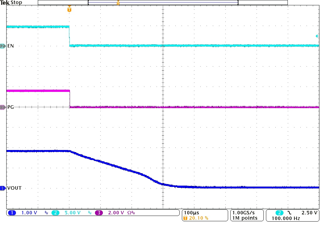
TA = 25°C, VIN = 5 V, VOUT = 1.8 V, BOM = Table 8-2 unless otherwise noted.

GUID-20221130-SS0I-XGLJ-V2TJ-HFSTBXKKP6BB-low.svg
VOUT = 3.3 V PFM
Figure 8-3 Efficiency versus Output Current
GUID-20221130-SS0I-RCRP-FQPJ-XQXMMKKJPRKD-low.svg
VOUT = 2.5 V PFM
Figure 8-5 Efficiency versus Output Current
GUID-20221130-SS0I-43XF-8CWF-SKKCFFXCBQ0R-low.svg
VOUT = 1.8 V PFM
Figure 8-7 Efficiency versus Output Current
GUID-20221130-SS0I-7N0N-7FGT-KWZQCDBLSMS1-low.svg
VOUT = 1.2 V PFM
Figure 8-9 Efficiency versus Output Current
GUID-20221130-SS0I-DTZN-ZHT6-QRLLL0BMZMLZ-low.svg
VOUT = 0.9 V PFM
Figure 8-11 Efficiency versus Output Current
GUID-20221130-SS0I-4L98-CNGS-TPGNXLJNX07Z-low.svg
VOUT = 0.5 V PFM TA = 25 °C
Figure 8-13 Efficiency versus Output Current
GUID-20230914-SS0I-HDCG-RBX6-HXZTH4TPWBJ0-low.svg
VOUT = 0.5 V PFM
Figure 8-15 Output Voltage versus Output Current
GUID-20230914-SS0I-F01R-FC36-099GSJJLTQCH-low.svg
VOUT = 0.9 V PFM
Figure 8-17 Output Voltage versus Output Current
GUID-20230914-SS0I-JDRX-QKBP-5PG5WHRXMWV1-low.svg
VOUT = 1.2 V PFM
Figure 8-19 Output Voltage versus Output Current
GUID-20230914-SS0I-GB9H-HLLL-D1Q7F8ZWTZMB-low.svg
VOUT = 1.8 V PFM
Figure 8-21 Output Voltage versus Output Current
GUID-20230914-SS0I-TC3S-D2K1-4X5HVMGLPPTL-low.svg
VOUT = 2.5 V PFM
Figure 8-23 Output Voltage versus Output Current
GUID-20230914-SS0I-17J8-WW2L-DKNW4HSM8KW9-low.svg
VOUT = 3.3 V PFM
Figure 8-25 Output Voltage versus Output Current
GUID-20231011-SS0I-VCSG-HVPG-RTZPHF1TW77H-low.svg
VIN = 3.3 V PFM
Figure 8-27 Switching Frequency versus Output Current
GUID-20231011-SS0I-JGWP-PBX3-XS6N288NJ676-low.svg
IOUT = 1 A
Figure 8-29 Switching Frequency versus Input Voltage
GUID-20221220-SS0I-D3TQ-ZW8N-NKFGFZ73LNPD-low.jpg
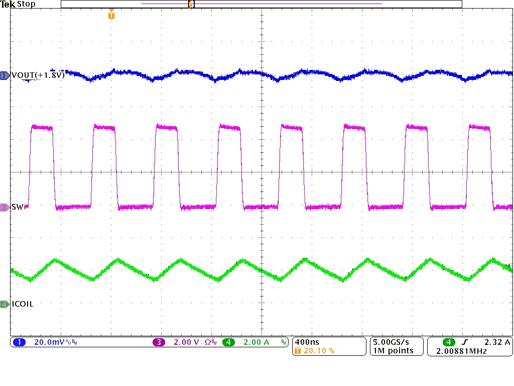
IOUT = 2.0 A PFM or PWM
Figure 8-31 Output Voltage Ripple
GUID-20221220-SS0I-2Z8S-3JQ5-GBLZCLMHWQJS-low.jpg
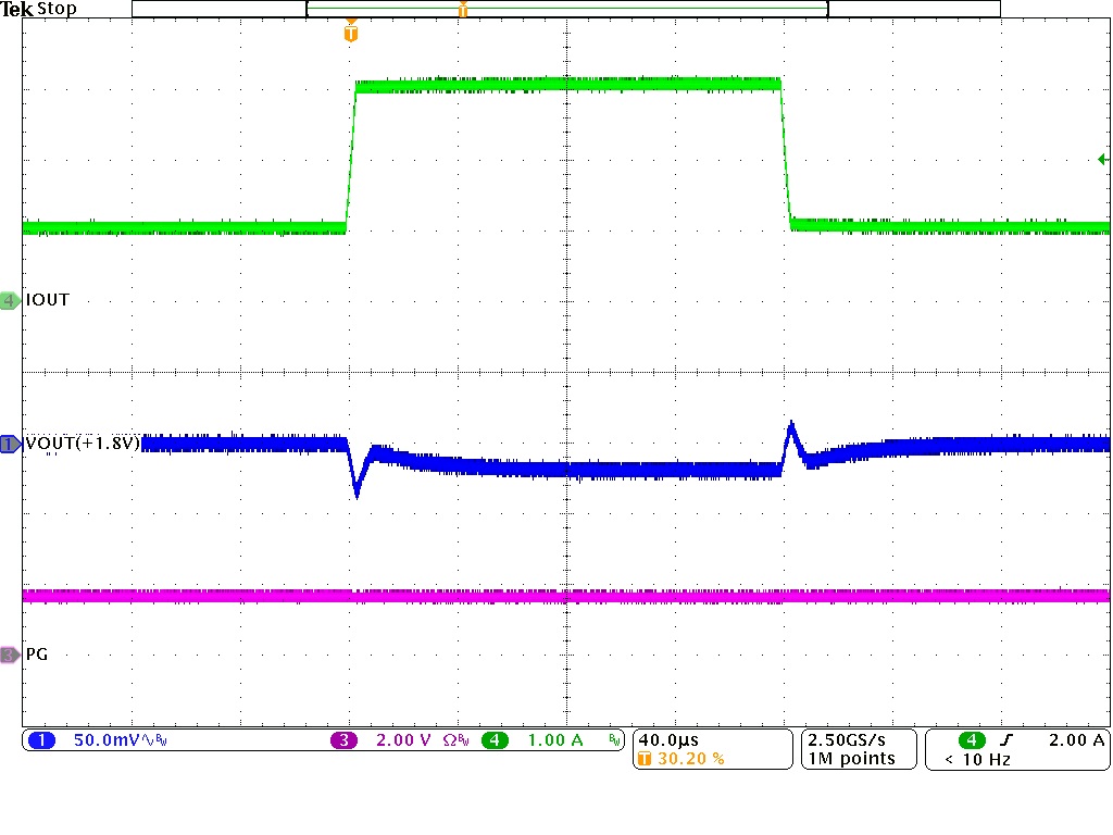
IOUT = 1 A to 3 A PWM Slew rate = 1 A/μs
Figure 8-33 Load Transient
GUID-20221220-SS0I-3FLX-ZTDP-5WLWNLSZHNFD-low.jpg
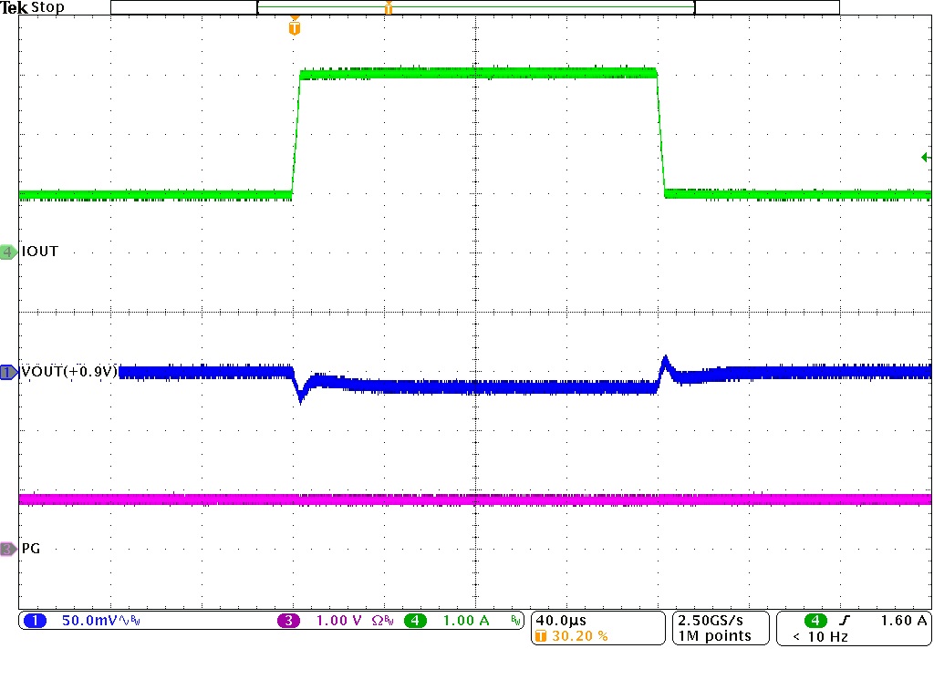
VIN = 3.3 V PWM IOUT = 1 A to 3 A
VOUT = 0.9 V Transient BoM Slew rate = 1 A/μs
Figure 8-35 Load Transient
GUID-20221220-SS0I-3NNJ-RMKJ-PSDLSMK6ZFFP-low.jpg
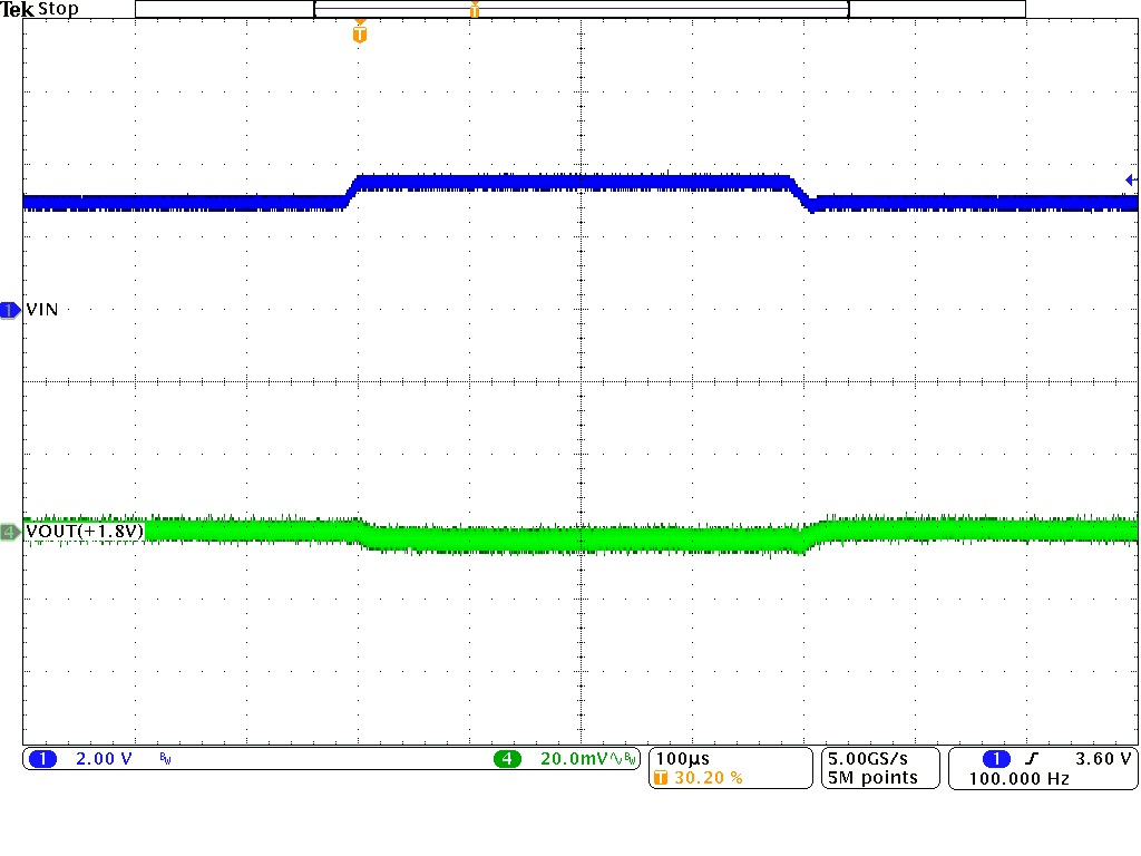
VIN = 4.5 V to 5.5 V PWM IOUT = 2.0 A
Figure 8-37 Line Transient
GUID-20221220-SS0I-LVQH-SB79-SK9BGLHS4SGL-low.jpg
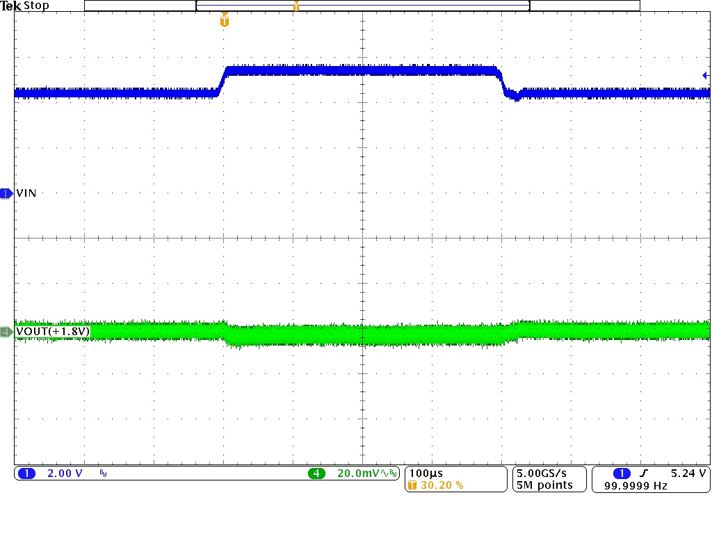
VIN = 3.0 V to 3.6 V PWM IOUT = 2.0 A
Figure 8-39 Line Transient
GUID-20221220-SS0I-HMJ0-3H4B-0QZCLKW3LPDQ-low.jpg
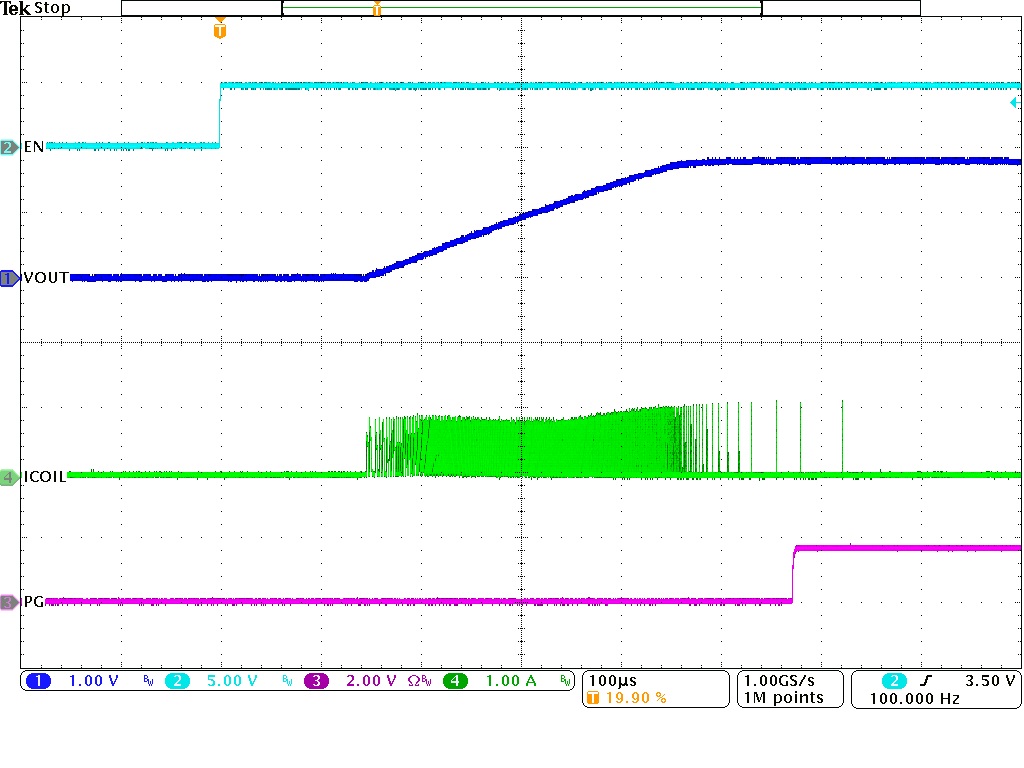
IOUT = 0 mA PFM or PWM TA = 25 °C
'A' and 'B' versions
Figure 8-41 Start-Up With No Load
GUID-20221220-SS0I-KPCH-SMCF-2F99ZJBBHTPT-low.jpg
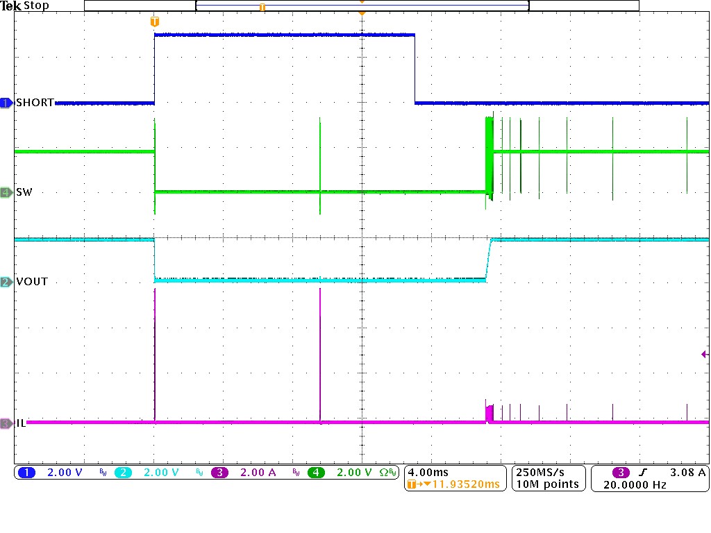
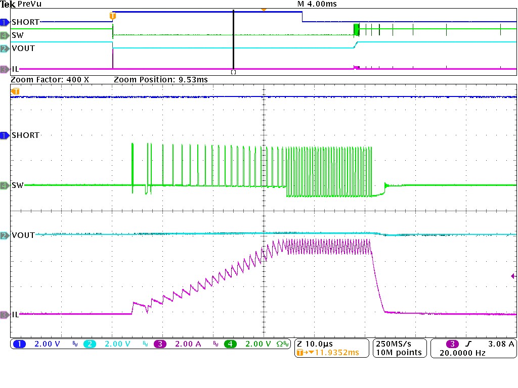
PFM or PWM TA = 25 °C
Figure 8-43 HICCUP Short-Circuit Protection
GUID-20221220-SS0I-FW4H-KRLV-TV9HDSNF4T09-low.jpg
PFM or PWM TA = 25 °C
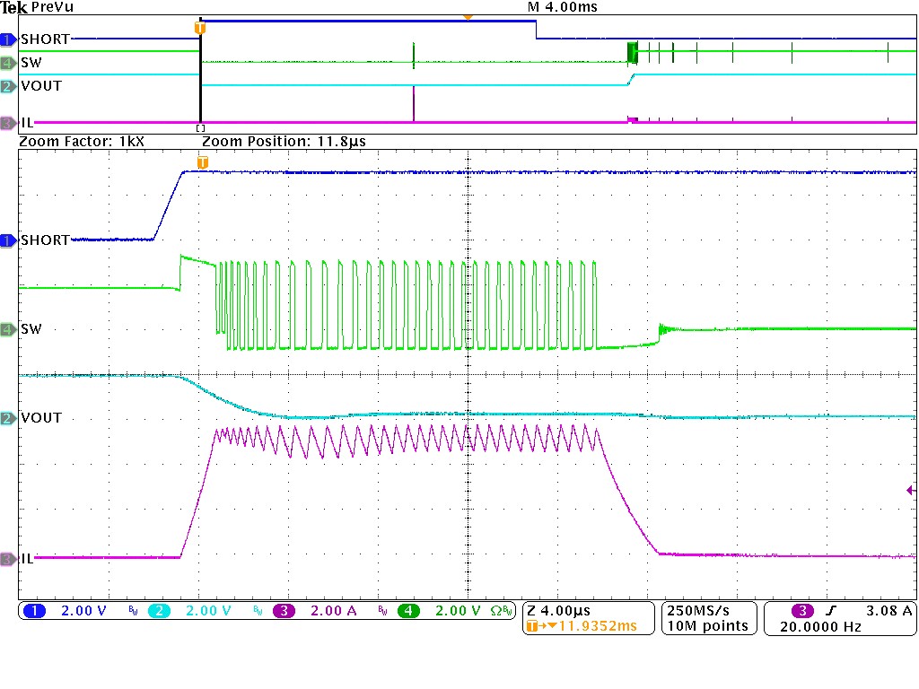
Figure 8-45 HICCUP Short-Circuit Protection (Zoom In - Second Hiccup)
GUID-20221220-SS0I-KHBM-F891-SMLCR71PHD7Z-low.jpg
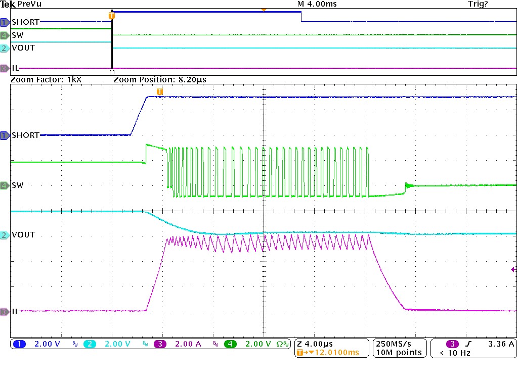
PFM or PWM TPS628303BDRL TA = 25 °C
Figure 8-47 Latch-off Short-Circuit Protection (Zoom In)
GUID-20221130-SS0I-3FCL-3B8M-6Q9XJPXQ3C5V-low.svg
VOUT = 3.3 V PWM
Figure 8-4 Efficiency versus Output Current
GUID-20221130-SS0I-BSD4-JNC1-2NNB313PRGHK-low.svg
VOUT = 2.5 V PWM
Figure 8-6 Efficiency versus Output Current
GUID-20221130-SS0I-H28K-G3MP-BZKDNZ271CWF-low.svg
VOUT = 1.8 V PWM
Figure 8-8 Efficiency versus Output Current
GUID-20221130-SS0I-LRLQ-TB1B-Z046WNQPQML5-low.svg
VOUT = 1.2 V PWM
Figure 8-10 Efficiency versus Output Current
GUID-20221130-SS0I-6GLB-1S3N-CQGPMVCKFVZ9-low.svg
VOUT = 0.9 V PWM
Figure 8-12 Efficiency versus Output Current
GUID-20221130-SS0I-GXWH-P0M1-2ZJN7XCDLX0F-low.svg
VOUT = 0.5 V PWM TA = 25 °C
Figure 8-14 Efficiency versus Output Current
GUID-20230914-SS0I-5CH1-12PR-FBLDBMRCMPCR-low.svg
VOUT = 0.5 V PWM
Figure 8-16 Output Voltage versus Output Current
GUID-20230914-SS0I-GXVG-H93G-1JWFGNMKJBRW-low.svg
VOUT = 0.9 V PWM
Figure 8-18 Output Voltage versus Output Current
GUID-20230914-SS0I-7KZ7-GZLC-FKMQ8FSZGB2J-low.svg
VOUT = 1.2 V PWM
Figure 8-20 Output Voltage versus Output Current
GUID-20230914-SS0I-86JQ-Z3MJ-GWDSC5HKLKZJ-low.svg
VOUT = 1.8 V PWM
Figure 8-22 Output Voltage versus Output Current
GUID-20230914-SS0I-1FQT-7JCB-KD1WZDCRNVDS-low.svg
VOUT = 2.5 V PWM
Figure 8-24 Output Voltage versus Output Current
GUID-20230914-SS0I-3PV5-ZPC4-8MZMGDLBRXPB-low.svg
VOUT = 3.3 V PWM
Figure 8-26 Output Voltage versus Output Current
GUID-20231011-SS0I-G5T5-5BVF-LTRBKVRNQP3B-low.svg
VIN = 3.3 V PWM
Figure 8-28 Switching Frequency versus Output Current
GUID-20221220-SS0I-TKQK-BSNQ-VVGHB1FV1QMJ-low.jpg
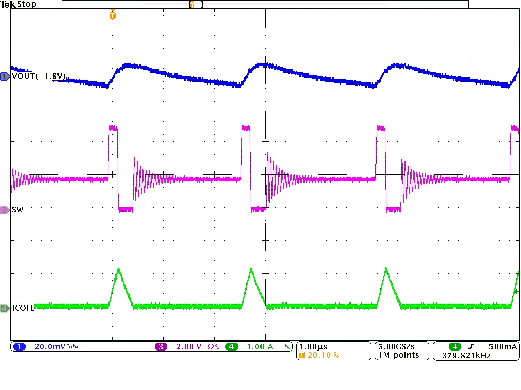
IOUT= 100 mA PFM
Figure 8-30 Output Voltage Ripple
GUID-20221220-SS0I-Z8NC-7XBN-SSJSMGSCZWRD-low.jpg
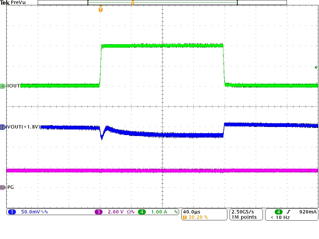
IOUT = 1 mA to 2 A PFM Slew rate = 1 A/μs
Figure 8-32 Load Transient
GUID-20221220-SS0I-D4WT-NCKK-CR7V5RVQLM4W-low.jpg
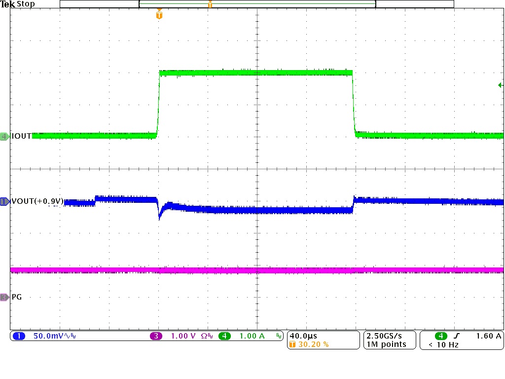
VIN = 3.3 V PFM IOUT = 1 mA to 2A
VOUT = 0.9 V Transient BoM Slew rate = 1 A/μs
Figure 8-34 Load Transient
GUID-20221220-SS0I-C1P6-DBWK-RQKRGNWVSK2H-low.jpg
VIN = 4.5 V to 5.5 V PFM IOUT = 100 mA
Figure 8-36 Line Transient
GUID-20221220-SS0I-GFK2-BLR2-DXBTCR7ZRJVJ-low.jpg
VIN = 3.0 V to 3.6 V PFM IOUT = 100 mA
Figure 8-38 Line Transient
GUID-20221220-SS0I-VH3F-RTFL-VHQW0WXVQVF4-low.jpg
IOUT = 2.0 A PFM or PWM TA = 25 °C
'A' and 'B' versions
Figure 8-40 Start-Up With Load
GUID-20221220-SS0I-LTCD-VXKK-TSK2GQ1ZZ5NP-low.jpg
IOUT = 0 mA PFM TA = 25 °C
Figure 8-42 Disable, Active Output Discharge at No Load
GUID-20221220-SS0I-FJR2-MGCX-HB2CNXXHTZJL-low.jpg
PFM or PWM TA = 25 °C
Figure 8-44 HICCUP Short-Circuit Protection (Zoom In)
GUID-20221220-SS0I-N7SD-QV7R-PFQBKKC47CVN-low.jpg
PFM or PWM TPS628303BDRL TA = 25 °C
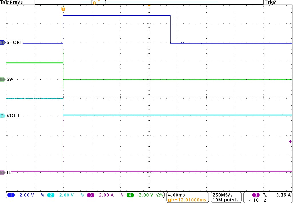
Figure 8-46 Latch-off Short-Circuit Protection
GUID-20221220-SS0I-HKCV-C4NL-2FM3LCLHJPQ3-low.jpg
PFM or PWM TPS628303BDRLR TA = 25 °C
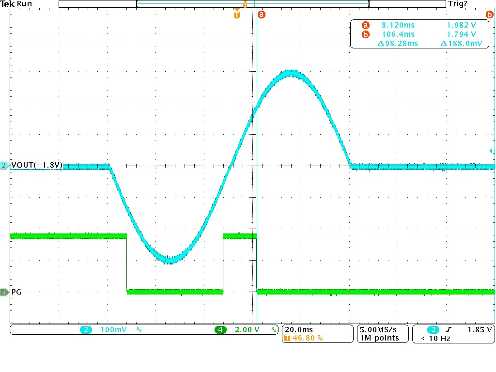
Figure 8-48 Latch-off Overvoltage Protection