SLVSFU8C January 2022 – June 2024 TPS62843
PRODUCTION DATA
- 1
- 1 Features
- 2 Applications
- 3 Description
- 4 Device Comparison Table
- 5 Pin Configuration and Functions
- 6 Specifications
- 7 Detailed Description
- 8 Application and Implementation
- 9 Device and Documentation Support
- 10Revision History
- 11Mechanical, Packaging, and Orderable Information
Package Options
Refer to the PDF data sheet for device specific package drawings
Mechanical Data (Package|Pins)
- DRL|6
- YKA|6
Thermal pad, mechanical data (Package|Pins)
Orderable Information
8.2.3 Application Curves
 Figure 8-2 Efficiency at
VOUT = 0.4V
 Figure 8-4 Efficiency at
VOUT = 1.2V
 Figure 8-6 Efficiency at
VOUT = 3.3V
 Figure 8-8 Output Voltage vs Output
Current at VOUT = 0.7V
 Figure 8-10 Switching Frequency vs
Output Current at VOUT = 0.7V
 Figure 8-12 Switching Frequency vs
Output Current at VOUT= 1.8V
 Figure 8-14 Typical Operation at
VOUT = 0.7V, IOUT = 100μA
 Figure 8-16 Typical Operation at
VOUT = 0.7V, IOUT = 400mA
 Figure 8-18 Load Transient at
VOUT = 0.7V, IOUT = 100μA to 400mA
  Figure 8-20 Load Transient at
VOUT = 1.2V, IOUT = 100μA to 20mA
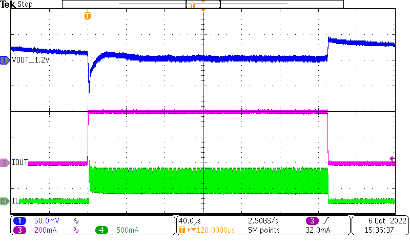
 Figure 8-22 Load Transient at
VOUT = 1.2V, IOUT = 5mA to 400mA
 Figure 8-24 AC Load Sweep at
VOUT = 1.2V, IOUT = 1mA to 600mA
 Figure 8-26 Line Transient at
VOUT = 1.2V, IOUT = 400mA, VIN = 3.6V
to 4.2V
 Figure 8-28 Start-Up Delay Time, VSET
= GND
 Figure 8-3 Efficiency at
VOUT = 0.7V
 Figure 8-5 Efficiency at
VOUT = 1.8V
 Figure 8-7 Output Voltage vs Output
Current at VOUT = 1.2V
 Figure 8-9 Switching Frequency vs
Output Current at VOUT = 0.4V
 Figure 8-11 Switching Frequency vs
Output Current at VOUT= 1.2V
 Figure 8-13 Power Supply Rejection
Ratio (PSRR) at VOUT = 1.8V
 Figure 8-15 Typical Operation at
VOUT = 0.7V, IOUT = 20mA
 Figure 8-17 Load Transient at
VOUT = 0.7V, IOUT = 100 μA to 20 mA
  Figure 8-19 Load Transient at
VOUT = 0.7V, IOUT = 5mA to 400mA
  Figure 8-21 Load Transient at
VOUT = 1.2V, IOUT = 100μA to 400mA
  Figure 8-23 AC Load Sweep at
VOUT = 0.7V, IOUT = 1mA to 600mA
 Figure 8-25 Line Transient at
VOUT = 0.7V, IOUT = 400mA, VIN = 3.6V
to 4.2V
 Figure 8-27 Shutdown, Output Discharge
at VOUT = 0.7V
 Figure 8-29 Start-Up Delay Time, VSET
= 10kohms