SLUSDO4B August 2020 – June 2022 TPS628510 , TPS628511 , TPS628512 , TPS628513
PRODUCTION DATA
- 1 Features
- 2 Applications
- 3 Description
- 4 Revision History
- 5 Device Comparison Table
- 6 Pin Configuration and Functions
- 7 Specifications
- 8 Parameter Measurement Information
-
9 Detailed Description
- 9.1 Overview
- 9.2 Functional Block Diagram
- 9.3 Feature Description
- 9.4
Device Functional Modes
- 9.4.1 Pulse Width Modulation (PWM) Operation
- 9.4.2 Power Save Mode Operation (PWM/PFM)
- 9.4.3 100% Duty-Cycle Operation
- 9.4.4 Current Limit and Short Circuit Protection
- 9.4.5 Foldback Current Limit and Short Circuit Protection
- 9.4.6 Output Discharge
- 9.4.7 Soft Start / Tracking (SS/TR)
- 9.4.8 Input Overvoltage Protection
- 10Application and Implementation
- 11Power Supply Recommendations
- 12Layout
- 13Device and Documentation Support
- 14Mechanical, Packaging, and Orderable Information
Package Options
Mechanical Data (Package|Pins)
- DRL|8
Thermal pad, mechanical data (Package|Pins)
Orderable Information
10.3.2 Synchronizing to an External Clock
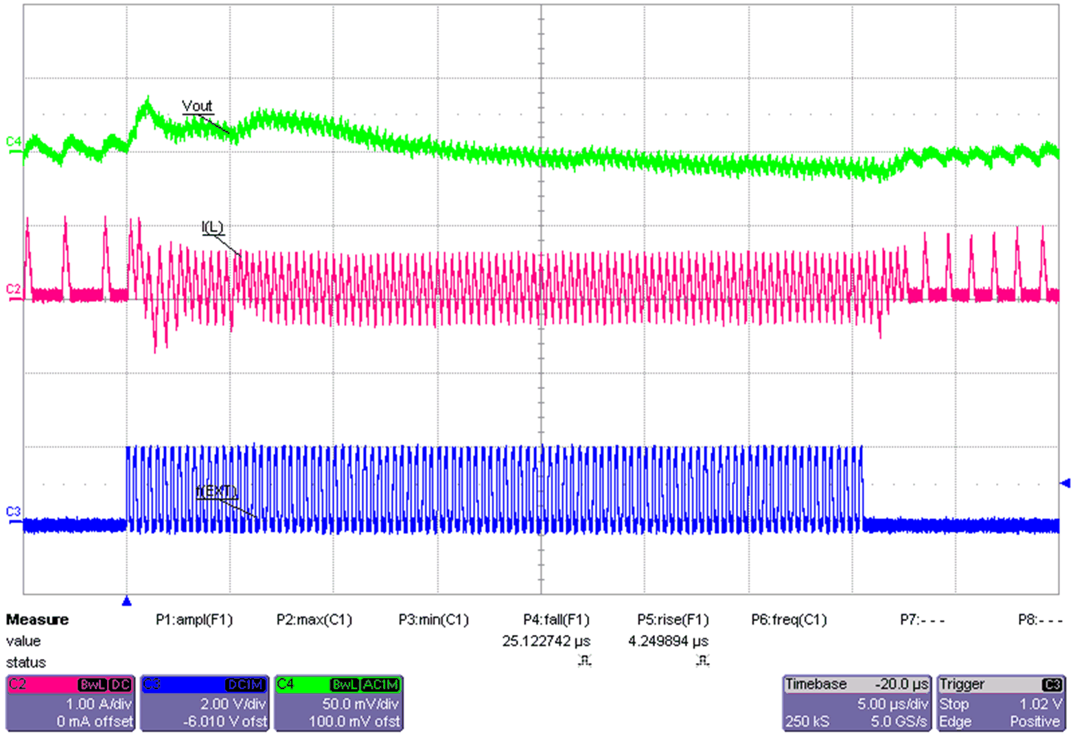
The TPS62851x can be externally synchronized by applying an external clock on the MODE/SYNC pin. There is no need for any additional circuitry as long as the input signal meets the requirements given in the electrical specifications. The clock can be applied / removed during operation, allowing you to switch from an externally defined fixed frequency to power-save mode or to internal fixed frequency operation.
 Figure 10-59 Schematic using External Synchronization
| VIN = 5 V | RCF = 8.06 kΩ | IOUT = 0.1 A |
| VOUT = 1.8 V | fEXT = 2.5 MHz |

| VIN = 5 V | RCF = 8.06 kΩ | IOUT = 0.1 A |
| VOUT = 1.8 V | fEXT = 2.5 MHz |