SLUSDU8F September 2019 – October 2023 TPS62860 , TPS62861
PRODUCTION DATA
- 1
- 1 Features
- 2 Applications
- 3 Description
- 4 Revision History
- 5 Device Comparison Table
- 6 Pin Configuration and Functions
- 7 Specifications
-
8 Detailed Description
- 8.1 Overview
- 8.2 Functional Block Diagram
- 8.3
Feature Description
- 8.3.1 Power Save Mode
- 8.3.2 Forced PWM Operation
- 8.3.3 Smart Enable and Shutdown (EN)
- 8.3.4 Soft Start
- 8.3.5 Output Voltage Selection (VSEL) for TPS62860x
- 8.3.6 Output Voltage Selection (VSEL and I2C)
- 8.3.7 Forced PWM Mode During Output Voltage Change
- 8.3.8 Undervoltage Lockout (UVLO)
- 8.3.9 Power Good (PG)
- 8.3.10 Switch Current Limit and Short Circuit Protection
- 8.3.11 Thermal Shutdown
- 8.3.12 Output Voltage Discharge
- 8.4 Programming
- 8.5 Register Map
- 9 Application and Implementation
- 10Device and Documentation Support
- 11Mechanical, Packaging, and Orderable Information
Package Options
Mechanical Data (Package|Pins)
- YCH|8
Thermal pad, mechanical data (Package|Pins)
Orderable Information
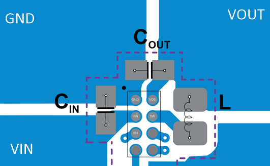
9.5.2 Layout Example
 Figure 9-20 PCB Layout Example