SLUSDU8G September   2019  – January 2025 TPS62860 , TPS62861

PRODUCTION DATA  

  1.   1
  2. Features
  3. Applications
  4. Description
  5. Device Comparison Table
  6. Pin Configuration and Functions
  7. Specifications
    1. 6.1 Absolute Maximum Ratings
    2. 6.2 ESD Ratings
    3. 6.3 Recommended Operating Conditions
    4. 6.4 Thermal Information
    5. 6.5 Electrical Characteristics
    6. 6.6 I2C Interface Timing Characteristics
    7. 6.7 Typical Characteristics
  8. Detailed Description
    1. 7.1 Overview
    2. 7.2 Functional Block Diagram
    3. 7.3 Feature Description
      1. 7.3.1 Soft Start
      2. 7.3.2 Output Voltage Selection (VSEL) for TPS62860x
      3. 7.3.3 Output Voltage Selection (VSEL and I2C)
      4. 7.3.4 Undervoltage Lockout (UVLO)
      5. 7.3.5 Power Good (PG)
      6. 7.3.6 Switch Current Limit and Short Circuit Protection
      7. 7.3.7 Thermal Shutdown
      8. 7.3.8 Output Voltage Discharge
    4. 7.4 Device Functional Modes
      1. 7.4.1 Smart Enable and Shutdown (EN)
      2. 7.4.2 Forced PWM Operation
      3. 7.4.3 Forced PWM Mode During Output Voltage Change
      4. 7.4.4 Power Save Mode
    5. 7.5 Programming
      1. 7.5.1 Serial Interface Description
      2. 7.5.2 Standard- and Fast-Mode Protocol
      3. 7.5.3 I2C Update Sequence
      4. 7.5.4 I2C Register Reset
  9. Register Map
    1. 8.1 I2C Address Byte
    2. 8.2 Register Address Byte
    3. 8.3 VOUT Register 1
    4. 8.4 VOUT Register 2
    5. 8.5 CONTROL Register
    6. 8.6 STATUS Register
  10. Application and Implementation
    1. 9.1 Application Information
    2. 9.2 Typical Application, TPS628610
      1. 9.2.1 Design Requirements
      2. 9.2.2 Detailed Design Procedure
        1. 9.2.2.1 Inductor Selection
        2. 9.2.2.2 Output Capacitor Selection
        3. 9.2.2.3 Input Capacitor Selection
      3. 9.2.3 Application Curves
    3. 9.3 Typical Application, TPS628600, TPS62860x
      1. 9.3.1 Design Requirements
      2. 9.3.2 Detailed Design Procedure
      3. 9.3.3 Application Curves
    4. 9.4 Power Supply Recommendations
    5. 9.5 Layout
      1. 9.5.1 Layout Guidelines
      2. 9.5.2 Layout Example
  11. 10Device and Documentation Support
    1. 10.1 Device Support
      1. 10.1.1 Third-Party Products Disclaimer
    2. 10.2 Receiving Notification of Documentation Updates
    3. 10.3 Support Resources
    4. 10.4 Trademarks
    5. 10.5 Electrostatic Discharge Caution
    6. 10.6 Glossary
  12. 11Revision History
  13. 12Mechanical, Packaging, and Orderable Information

Package Options

Mechanical Data (Package|Pins)
Thermal pad, mechanical data (Package|Pins)
Orderable Information

Description

The TPS6286x devices are high-frequency, synchronous step-down converters with I2C- and VSEL-Interface. The devices provide an efficient, flexible, and high-power density point-of-load DC/DC design. At medium to heavy loads, the converter operates in PWM mode and automatically enters Power Save Mode operation at light load to maintain high efficiency over the entire load current range. The device can also be forced in PWM mode operation for the smallest output voltage ripple. Together, with the DCS-Control architecture, excellent load transient performance and tight output voltage accuracy are achieved. With the I2C interface and a dedicated VSEL pin, the output voltage is quickly adjusted to adapt the power consumption of the load to the ever-changing performance needs of the application. The device family is available with two VSEL pins and four factory preset voltages to allow usage without I2C interface.

Device Information
PART NUMBER(3) CURRENT PACKAGE(1) PACKAGE SIZE(2)
TPS62861 1A YCH (DSBGA, 8) 1.40mm × 0.70mm
TPS62860 0.6A
For more information, see Section 12.
The package size (length × width) is a nominal value and includes pins, where applicable.
TPS62860 TPS62861 Typical ApplicationTypical Application
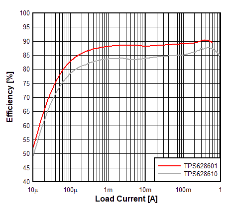
TPS62860 TPS62861 Efficiency vs IOUT at
                            1.1VOUT, 3.8VINEfficiency vs IOUT at 1.1VOUT, 3.8VIN