SLVSFM1A March 2021 – November 2023 TPS62902
PRODUCTION DATA
- 1
- 1 Features
- 2 Applications
- 3 Description
- 4 Revision History
- 5 Pin Configuration and Functions
- 6 Specifications
-
7 Detailed Description
- 7.1 Overview
- 7.2 Functional Block Diagram
- 7.3
Feature Description
- 7.3.1 Mode Selection and Device Configuration MODE/S-CONF
- 7.3.2 Adjustable VO Operation (External Voltage Divider)
- 7.3.3 Setable VO Operation (VSET and Internal Voltage Divider)
- 7.3.4 Soft Start / Tracking (SS/TR)
- 7.3.5 Smart Enable with Precise Threshold
- 7.3.6 Power Good (PG)
- 7.3.7 Undervoltage Lockout (UVLO)
- 7.3.8 Current Limit And Short Circuit Protection
- 7.3.9 Thermal Shutdown
- 7.4 Device Functional Modes
-
8 Application and Implementation
- 8.1 Application Information
- 8.2
Typical Application with Adjustable Output Voltage
- 8.2.1 Design Requirements
- 8.2.2 Detailed Design Procedure
- 8.2.3 Application Curves
- 8.2.4 Typical Application with Setable VO using VSET
- 8.3 System Examples
- 8.4 Power Supply Recommendations
- 8.5 Layout
- 9 Device and Documentation Support
- 10Mechanical, Packaging, and Orderable Information
Package Options
Mechanical Data (Package|Pins)
- RPJ|9
Thermal pad, mechanical data (Package|Pins)
Orderable Information
7.3.1 Mode Selection and Device Configuration MODE/S-CONF
With MODE/S-CONF (SmartConfig), this device features an input with two functions. It can be used to customize the device behavior in two ways:
- Select the device mode (FPWM or auto PFM/PWM with AEE operation) traditionally with a HIGH- or LOW-level.
- Select the device configuration (switching frequency, internal/external feedback, output discharge, and PFM/PWM mode) by connecting a single resistor to the MODE/S-CONF pin.
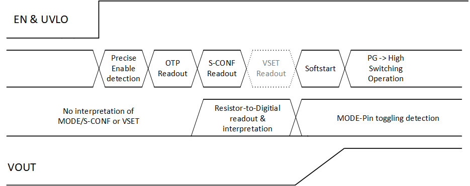
The device interprets this pin during the start-up sequence after the internal OTP readout and before it starts switching in soft start. If the device reads a HIGH- or LOW-level, the Dynamic Mode Change is active and PFM/PWM mode can be changed during operation. If the device reads a resistor value, there is no further interpretation during operation and device mode or other configurations cannot be changed afterwards.
Note: The MODE/S-CONF pin must not be left
floating. Connect the pin high, low, or to a resistor to configure the device according to
Table 7-1.
 Figure 7-1 Interpretation of S-CONF and VSET
Flow
Figure 7-1 Interpretation of S-CONF and VSET
FlowTable 7-1 SmartConfig Setting Table
| # | LEVEL OR RESISTOR VALUE [Ω] (1) | FB/VSET-PIN | FSW (MHz) | OUTPUT DISCHARGE | MODE (AUTO OR FORCED PWM) | DYNAMIC MODE CHANGE |
|---|---|---|---|---|---|---|
| Setting Options by Level | ||||||
| 1 | GND | external FB | 2.5 | yes | Auto PFM/PWM with AEE | active |
| 2 | HIGH (>VIH_MODE) | external FB | 2.5 | yes | Forced PWM | |
| Setting Options by Resistor | ||||||
| 3 | 7.15 k | external FB | 2.5 | no | Auto PFM/PWM with AEE | not active |
| 4 | 8.87 k | external FB | 2.5 | no | Forced PWM | |
| 5 | 11.0 k | external FB | 1 | yes | Auto PFM/PWM | |
| 6 | 13.7 k | external FB | 1 | yes | Forced PWM | |
| 7 | 16.9 k | external FB | 1 | no | Auto PFM/PWM | |
| 8 | 21.0 k | external FB | 1 | no | Forced PWM | |
| 9 | 26.1 k | VSET | 2.5 | yes | Auto PFM/PWM with AEE | |
| 10 | 32.4 k | VSET | 2.5 | yes | Forced PWM | |
| 11 | 40.2 k | VSET | 2.5 | no | Auto PFM/PWM with AEE | |
| 12 | 49.9 k | VSET | 2.5 | no | Forced PWM | |
| 13 | 61.9 k | VSET | 1 | yes | Auto PFM/PWM | |
| 14 | 76.8 k | VSET | 1 | yes | Forced PWM | |
| 15 | 95.3 k | VSET | 1 | no | Auto PFM/PWM | |
| 16 | 118 k | VSET | 1 | no | Forced PWM | |
(1) E96 Resistor Series, 1% Accuracy,
Temperature Coefficient better or equal than ±200 ppm/°C