SLVSFM1A March 2021 – November 2023 TPS62902
PRODUCTION DATA
- 1
- 1 Features
- 2 Applications
- 3 Description
- 4 Revision History
- 5 Pin Configuration and Functions
- 6 Specifications
-
7 Detailed Description
- 7.1 Overview
- 7.2 Functional Block Diagram
- 7.3
Feature Description
- 7.3.1 Mode Selection and Device Configuration MODE/S-CONF
- 7.3.2 Adjustable VO Operation (External Voltage Divider)
- 7.3.3 Setable VO Operation (VSET and Internal Voltage Divider)
- 7.3.4 Soft Start / Tracking (SS/TR)
- 7.3.5 Smart Enable with Precise Threshold
- 7.3.6 Power Good (PG)
- 7.3.7 Undervoltage Lockout (UVLO)
- 7.3.8 Current Limit And Short Circuit Protection
- 7.3.9 Thermal Shutdown
- 7.4 Device Functional Modes
-
8 Application and Implementation
- 8.1 Application Information
- 8.2
Typical Application with Adjustable Output Voltage
- 8.2.1 Design Requirements
- 8.2.2 Detailed Design Procedure
- 8.2.3 Application Curves
- 8.2.4 Typical Application with Setable VO using VSET
- 8.3 System Examples
- 8.4 Power Supply Recommendations
- 8.5 Layout
- 9 Device and Documentation Support
- 10Mechanical, Packaging, and Orderable Information
Package Options
Mechanical Data (Package|Pins)
- RPJ|9
Thermal pad, mechanical data (Package|Pins)
Orderable Information
8.3.2 Powering Multiple Loads
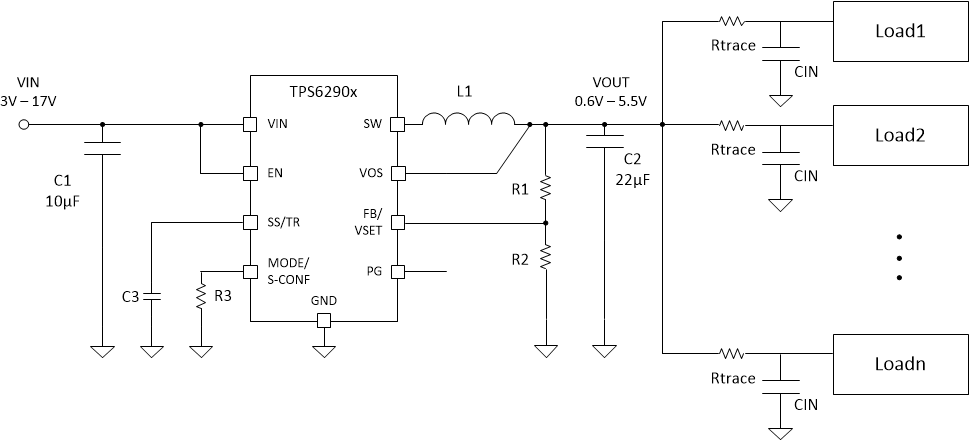
In applications where the TPS62902 is used to power multiple load circuits, the total capacitance on the output can be very large. In order to properly regulate the output voltage, there needs to be an appropriate AC signal level on the VOS pin. Tantalum capacitors have a large enough ESR to keep output voltage ripple sufficiently high on the VOS pin. With low-ESR ceramic capacitors, the output voltage ripple can get very low, so it is not recommended to use a large capacitance directly on the output of the device. If there are several load circuits with their associated input capacitor on a pcb, these loads are typically distributed across the board. This adds enough trace resistance (Rtrace) to keep a large enough AC signal on the VOS pin for proper regulation.
The minimum total trace resistance on the distributed load is 10 mΩ. The total capacitance n x CIN in the use case below was 32 × 47 μF of ceramic X7R capacitors.
 Figure 8-83 Multiple
Loads