SLVSFP4B August 2020 – March 2021 TPS62912 , TPS62913
PRODUCTION DATA
- 1 Features
- 2 Applications
- 3 Description
- 4 Revision History
- 5 Pin Configuration and Functions
- 6 Specifications
-
7 Detailed Description
- 7.1 Overview
- 7.2 Functional Block Diagram
- 7.3
Feature Description
- 7.3.1 Smart Config (S-CONF)
- 7.3.2 Device Enable (EN/SYNC)
- 7.3.3 Device Synchronization (EN/SYNC)
- 7.3.4 Spread Spectrum Modulation
- 7.3.5 Output Discharge
- 7.3.6 Undervoltage Lockout (UVLO)
- 7.3.7 Power-Good Output
- 7.3.8 Noise Reduction and Soft-Start Capacitor (NR/SS)
- 7.3.9 Current Limit and Short Circuit Protection
- 7.3.10 Thermal Shutdown
- 7.4 Device Functional Modes
- 8 Application and Implementation
- 9 Power Supply Recommendations
- 10Layout
- 11Device and Documentation Support
- 12Mechanical, Packaging, and Orderable Information
Package Options
Mechanical Data (Package|Pins)
- RPU|10
Thermal pad, mechanical data (Package|Pins)
Orderable Information
7.3.3 Device Synchronization (EN/SYNC)
The EN/SYNC pin is also used for device synchronization. Once a clock signal is applied to this pin, the device is enabled and reads the configuration of the S-CONF pin. The external clock frequency must be within the clock synchronization frequency range set by the S-CONF pin. When the clock signal changes from a clock to a static high, then the device switches from external clock to internal clock. To shutdown the device when using an external clock, EN/SYNC must go low for at least 10 µs.
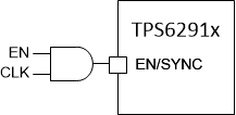
The clock signal can be a logic signal with a logic level as specified in the electrical table, and can be applied directly to the EN/SYNC pin. External logic, such as an AND gate, can be used to combine separate enable and clock inputs, as shown in Figure 7-1.
 Figure 7-1 Synchronization with Separate Enable Signal (optional)