SLVSG94C November 2023 – June 2024 TPS62914 , TPS62916 , TPS62918
PRODUCTION DATA
- 1
- 1 Features
- 2 Applications
- 3 Description
- 4 Pin Configuration and Functions
- 5 Specifications
-
6 Detailed Description
- 6.1 Overview
- 6.2 Functional Block Diagram
- 6.3
Feature Description
- 6.3.1 Smart Config (S-CONF)
- 6.3.2 Device Enable (EN/SYNC)
- 6.3.3 Device Synchronization (EN/SYNC)
- 6.3.4 Spread Spectrum Modulation
- 6.3.5 Output Discharge
- 6.3.6 Undervoltage Lockout (UVLO)
- 6.3.7 Power-Good Output
- 6.3.8 Noise Reduction and Soft-Start Capacitor (NR/SS)
- 6.3.9 Current Limit and Short-Circuit Protection
- 6.3.10 Thermal Shutdown
- 6.4 Device Functional Modes
-
7 Application and Implementation
- 7.1 Application Information
- 7.2
Typical Applications
- 7.2.1 Design Requirements
- 7.2.2
Detailed Design Procedure
- 7.2.2.1 Custom Design With WEBENCH® Tools
- 7.2.2.2
External Component Selection
- 7.2.2.2.1 Switching Frequency Selection
- 7.2.2.2.2 Inductor Selection for the First L-C Filter
- 7.2.2.2.3 Output Capacitor Selection
- 7.2.2.2.4 Ferrite Bead Selection for Second L-C Filter
- 7.2.2.2.5 Input Capacitor Selection
- 7.2.2.2.6 Setting the Output Voltage
- 7.2.2.2.7 Bootstrap Capacitor Selection
- 7.2.2.2.8 NR/SS Capacitor Selection
- 7.2.3 Application Curves
- 7.3 Power Supply Recommendations
- 7.4 Layout
- 8 Device and Documentation Support
- 9 Revision History
- 10Mechanical, Packaging, and Orderable Information
Package Options
Mechanical Data (Package|Pins)
- RPY|14
Thermal pad, mechanical data (Package|Pins)
Orderable Information
6.3.4 Spread Spectrum Modulation
Using the S-CONF pin enables or disables spread spectrum modulation. DC/DC converter generate an output voltage ripple at the switching frequency. When powering ADCs or an analog front-end (AFE), the switching frequency generates high frequency mixing spurs as well as a low frequency spur in the output frequency spectrum. Using the optional second stage L-C filter reduces the ripple of the converter and spurs by up to 30 dB.
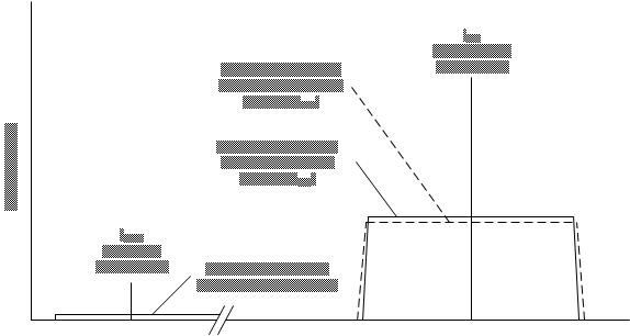
The device has an integrated random spread spectrum modulation (SSM) scheme, selected by the resistor connected to the S-CONF pin according to Table 6-1. Selecting random modulation to spread the switching frequency over a larger frequency range is possible. The modulation spread is +/– 10% of the device switching frequency. This SSM provides high attenuation when the receiver bandwidth is ≤ the modulation frequency, typically the case for systems using Fast Fourier Transforms (FFT) post processing as in high speed ADC applications. For applications sensitive to noise at the modulation frequency, random SSM is used. Using a random spread spectrum modulation also reduces the spurs in the output spectrum as shown in Figure 5-2. The randomized modulation uses a Fibonacci Linear-Feedback Shift Register (LFSR) so that every tone is generated once during the pseudo-random generation period. The frequency spreading is shown in Figure 6-2..
 Figure 6-2 Spread Spectrum Modulation