SLVSG94C November 2023 – June 2024 TPS62914 , TPS62916 , TPS62918
PRODUCTION DATA
- 1
- 1 Features
- 2 Applications
- 3 Description
- 4 Pin Configuration and Functions
- 5 Specifications
-
6 Detailed Description
- 6.1 Overview
- 6.2 Functional Block Diagram
- 6.3
Feature Description
- 6.3.1 Smart Config (S-CONF)
- 6.3.2 Device Enable (EN/SYNC)
- 6.3.3 Device Synchronization (EN/SYNC)
- 6.3.4 Spread Spectrum Modulation
- 6.3.5 Output Discharge
- 6.3.6 Undervoltage Lockout (UVLO)
- 6.3.7 Power-Good Output
- 6.3.8 Noise Reduction and Soft-Start Capacitor (NR/SS)
- 6.3.9 Current Limit and Short-Circuit Protection
- 6.3.10 Thermal Shutdown
- 6.4 Device Functional Modes
-
7 Application and Implementation
- 7.1 Application Information
- 7.2
Typical Applications
- 7.2.1 Design Requirements
- 7.2.2
Detailed Design Procedure
- 7.2.2.1 Custom Design With WEBENCH® Tools
- 7.2.2.2
External Component Selection
- 7.2.2.2.1 Switching Frequency Selection
- 7.2.2.2.2 Inductor Selection for the First L-C Filter
- 7.2.2.2.3 Output Capacitor Selection
- 7.2.2.2.4 Ferrite Bead Selection for Second L-C Filter
- 7.2.2.2.5 Input Capacitor Selection
- 7.2.2.2.6 Setting the Output Voltage
- 7.2.2.2.7 Bootstrap Capacitor Selection
- 7.2.2.2.8 NR/SS Capacitor Selection
- 7.2.3 Application Curves
- 7.3 Power Supply Recommendations
- 7.4 Layout
- 8 Device and Documentation Support
- 9 Revision History
- 10Mechanical, Packaging, and Orderable Information
Package Options
Mechanical Data (Package|Pins)
- RPY|14
Thermal pad, mechanical data (Package|Pins)
Orderable Information
7.2.3 Application Curves
VIN = 12 V, VOUT = 1.2 V, TA = 25°C, BOM = Table 7-1

| 0.8 Vout | 1 μH, 1 MHz | 1st L-C Only |

| 1.8 Vout | 1 μH, 1.4 MHz | 1st L-C Only |

| 5.0 Vout | 1 μH, 2.2 MHz | 1st L-C Only |

| 1.8 Vout | 1 μH, 1.4 MHz | 1st L-C Only |
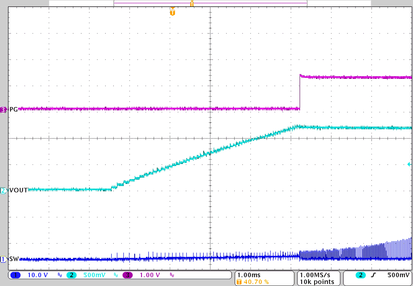
NR/SS = 470 nF
Figure 7-10 Start-up| 12 V to 1.2 V | 1 μH, 1 MHz | 1 A Load |
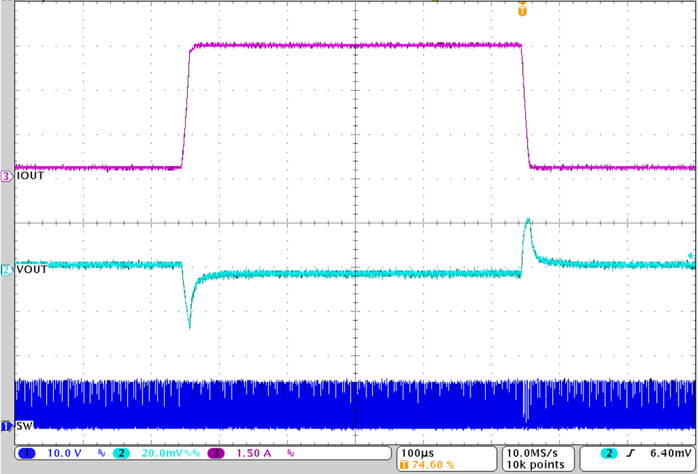
300 mA to 4.5 A to 300 mA
Figure 7-12 Load Transient| 12 V to 1.2 V | 1 μH, 1 MHz | 1st L-C Only |
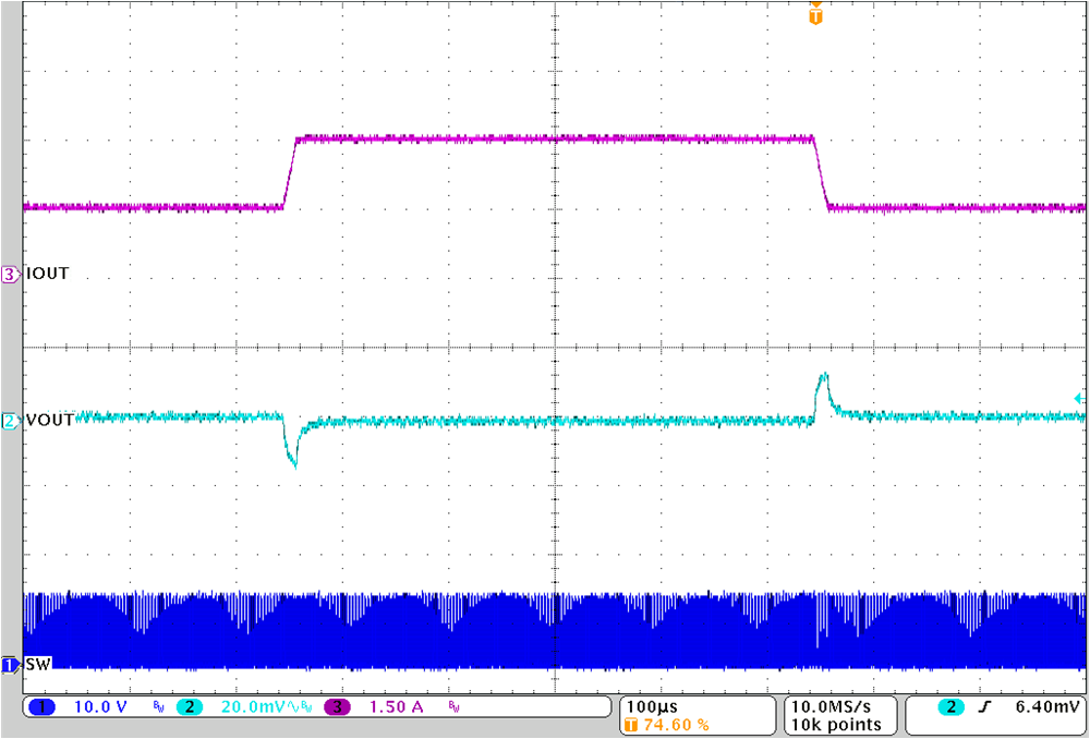
1.5 A to 3 A to 1.5 A
Figure 7-14 Load Transient| 12 V to 1.2 V | 1 μH, 1 MHz | After 2nd L-C |

300 mA to 4.5 A to 300 mA
Figure 7-16 Load Transient| 12 V to 1.2 V | 1 μH, 1 MHz | 1st L-C Only |

300 mA to 4.5 A to 300 mA
Figure 7-18 Load Transient| 12 V to 1.8 V | 1 μH, 1 MHz | 1st L-C Only |
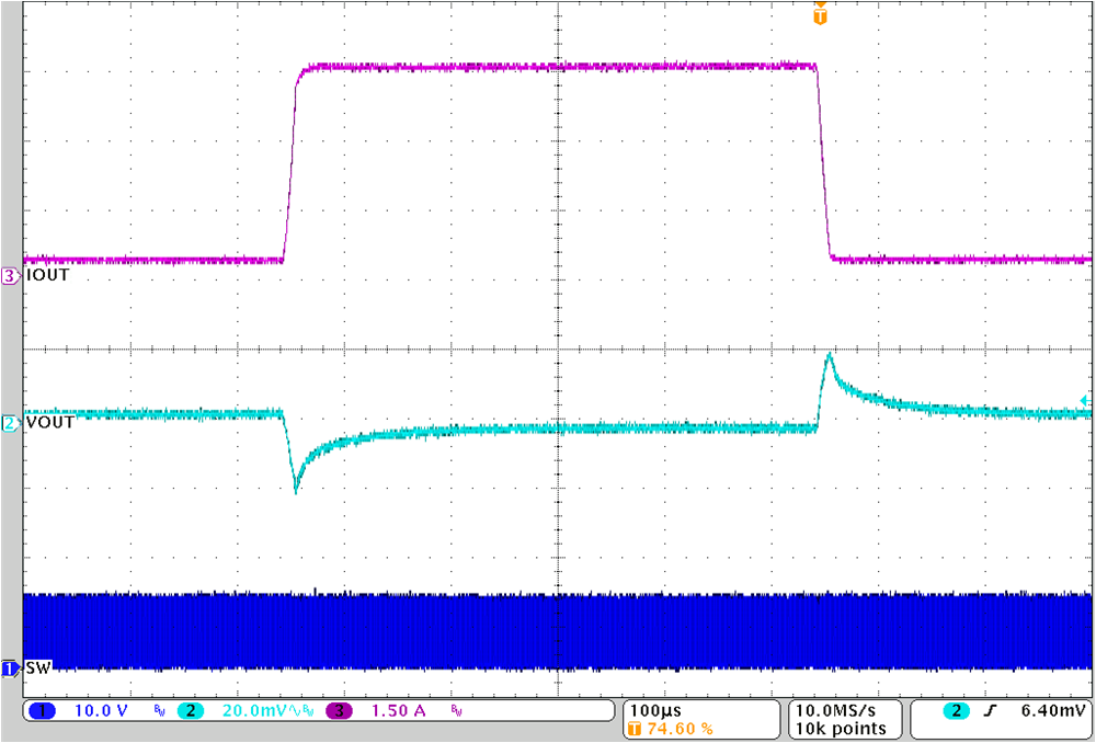
300 mA to 4.5 A to 300 mA
Figure 7-20 Load Transient| 12 V to 3.3 V | 1 μH, 2.2 MHz | 1st L-C Only |

| 1.2 Vout | 1 μH, 1 MHz | 1st L-C Only |

| 3.3 Vout | 1 μH, 2.2 MHz | 1st L-C Only |

| 1.2 Vout | 1 μH, 1 MHz | 1st L-C Only |

| 3.3 Vout | 1 μH, 2.2 MHz | 1st L-C Only |
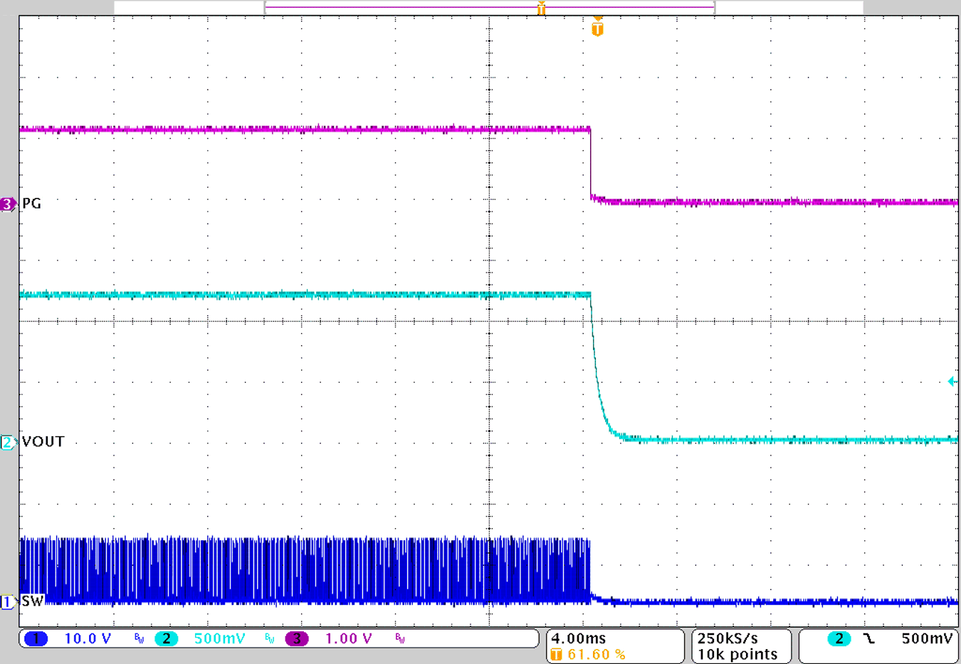
NR/SS = 470 nF
Figure 7-11 Shutdown| 12 V to 1.2 V | 1 μH, 1 MHz | 0 A Load, Discharge On |
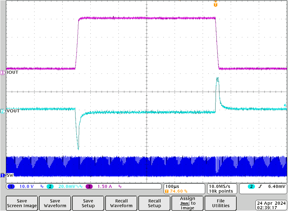
300 mA to 4.5 A to 300 mA
Figure 7-13 Load Transient| 12 V to 1.2 V | 1 μH, 1 MHz | After 2nd L-C |
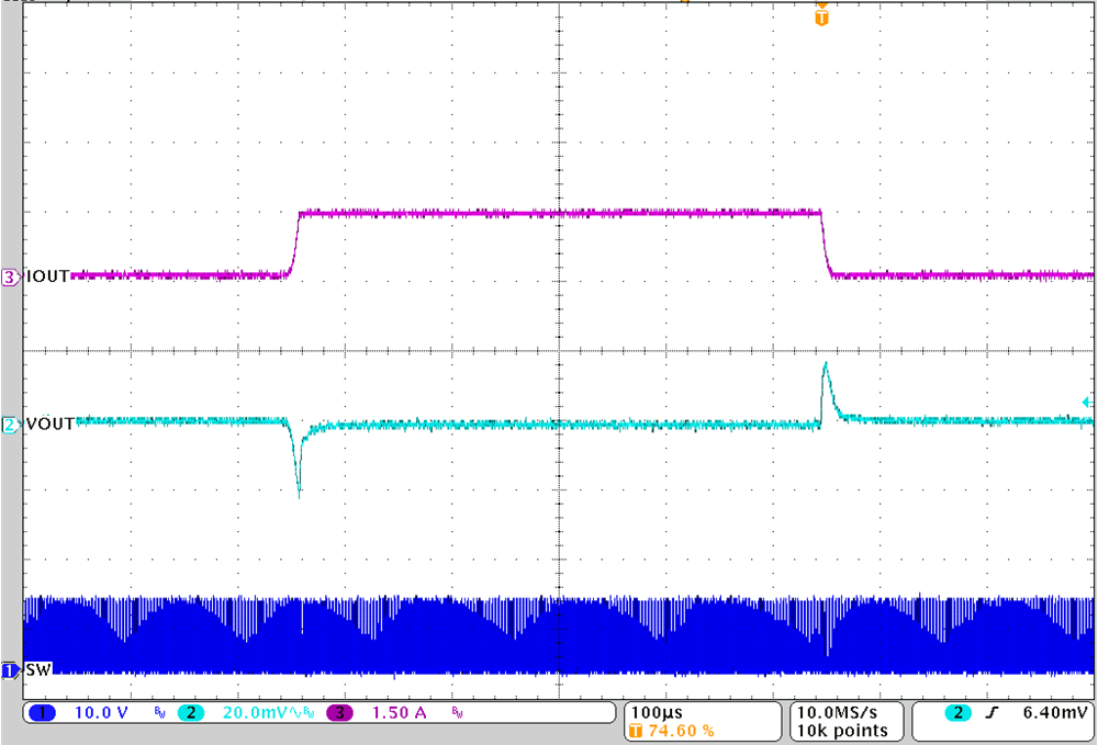
30 mA to 1.5 A to 30 mA
Figure 7-15 Load Transient| 12 V to 1.2 V | 1 μH, 1 MHz | After 2nd L-C |

300 mA to 4.5 A to 300 mA
Figure 7-17 Load Transient| 12 V to 1.2 V | 1 μH, 1 MHz | After 2nd L-C |
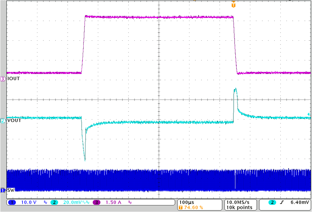
300 mA to 4.5 A to 300 mA
Figure 7-19 Load Transient| 12 V to 1.8 V | 1 μH, 1 MHz | After 2nd L-C |
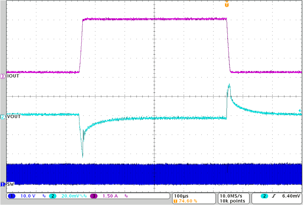
300 mA to 4.5 A to 300 mA
Figure 7-21 Load Transient| 12 V to 3.3 V | 1 μH, 2.2 MHz | After 2nd L-C |