SLVSGE1 March 2022 TPS629206
PRODUCTION DATA
- 1 Features
- 2 Applications
- 3 Description
- 4 Revision History
- 5 Device Comparison Table
- 6 Pin Configuration and Functions
- 7 Specifications
-
8 Detailed Description
- 8.1 Overview
- 8.2 Functional Block Diagram
- 8.3
Feature Description
- 8.3.1 Mode Selection and Device Configuration (MODE/S-CONF Pin)
- 8.3.2 Adjustable VO Operation (External Voltage Divider)
- 8.3.3 Selectable VO Operation (VSET and Internal Voltage Divider)
- 8.3.4 Smart Enable with Precise Threshold
- 8.3.5 Power Good (PG)
- 8.3.6 Output Discharge Function
- 8.3.7 Undervoltage Lockout (UVLO)
- 8.3.8 Current Limit and Short Circuit Protection
- 8.3.9 Thermal Shutdown
- 8.4 Device Functional Modes
- 9 Application and Implementation
- 10Power Supply Recommendations
- 11Layout
- 12Device and Documentation Support
- 13Mechanical, Packaging, and Orderable Information
Package Options
Mechanical Data (Package|Pins)
- DRL|8
Thermal pad, mechanical data (Package|Pins)
Orderable Information
8.3.3 Selectable VO Operation (VSET and Internal Voltage Divider)
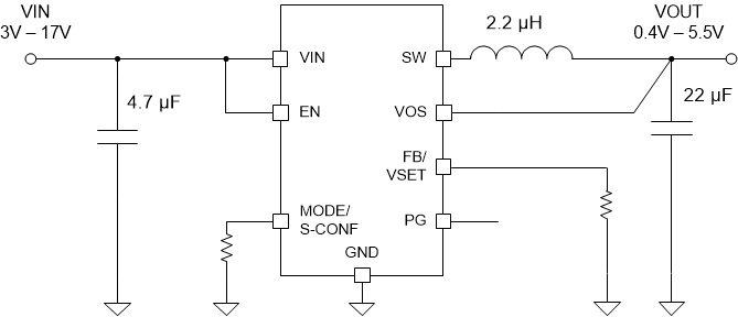
If the device is configured to VSET operation, the device interprets the VSET pin value following the MODE/S-CONF readout (see Figure 8-3). There is no further interpretation of the VSET pin during operation and the output voltage cannot be changed afterward without toggling the EN pin.
Figure 8-3 shows the typical schematic for this configuration, where VO is directly sensed at the VOS pin of the device. VO is sensed only through the VOS pin by an internal resistor divider. The target VO is programmed by an external resistor connected between VSET and GND (see Table 8-2).
 Figure 8-3 Selectable VO Operation
Schematic
 Table 8-2 VSET Selection Table
| VSET # | Resistor Value [Ω](1) | Target VO [V] |
|---|---|---|
| 1 | GND | 1.2 |
| 2 | 4.87 k | 0.4 |
| 3 | 6.04 k | 0.6 |
| 4 | 7.50 k | 0.8 |
| 5 | 9.31 k | 0.85 |
| 6 | 11.50 k | 1.0 |
| 7 | 14.30 k | 1.1 |
| 8 | 17.80 k | 1.25 |
| 9 | 22.10 k | 1.3 |
| 10 | 27.40 k | 1.35 |
| 11 | 34.00 k | 1.8 |
| 12 | 42.20 k | 1.9 |
| 13 | 52.30 k | 2.5 |
| 14 | 64.90 k | 3.8 |
| 15 | 80.60 k | 5.0 |
| 16 | 100.00 k | 5.1 |
| 17 | 124.00 k | 5.5 |
| 18 | 249.00 k or larger/open | 3.3 |
(1) E96 Resistor Series, 1% accuracy,
temperature coefficient better or equal to ±200 ppm/°C