SLVSHX6 December 2024 TPS62964 , TPS62966 , TPS62968
PRODUCTION DATA
- 1
- 1 Features
- 2 Applications
- 3 Description
- 4 Pin Configuration and Functions
- 5 Specifications
-
6 Detailed Description
- 6.1 Overview
- 6.2 Functional Block Diagram
- 6.3
Feature Description
- 6.3.1 Smart Config (S-CONF)
- 6.3.2 Device Enable (EN/SYNC)
- 6.3.3 Device Synchronization (EN/SYNC)
- 6.3.4 Spread Spectrum Modulation
- 6.3.5 Output Discharge
- 6.3.6 Undervoltage Lockout (UVLO)
- 6.3.7 Power-Good Output
- 6.3.8 Noise Reduction and Soft-Start Capacitor (NR/SS)
- 6.3.9 Current Limit and Short-Circuit Protection
- 6.3.10 Thermal Shutdown
- 6.4 Device Functional Modes
-
7 Application and Implementation
- 7.1 Application Information
- 7.2
Typical Applications
- 7.2.1 Design Requirements
- 7.2.2
Detailed Design Procedure
- 7.2.2.1 Custom Design With WEBENCH® Tools
- 7.2.2.2
External Component Selection
- 7.2.2.2.1 Switching Frequency Selection
- 7.2.2.2.2 Inductor Selection for the First L-C Filter
- 7.2.2.2.3 Output Capacitor Selection
- 7.2.2.2.4 Ferrite Bead Selection for Second L-C Filter
- 7.2.2.2.5 Input Capacitor Selection
- 7.2.2.2.6 Setting the Output Voltage
- 7.2.2.2.7 Bootstrap Capacitor Selection
- 7.2.2.2.8 NR/SS Capacitor Selection
- 7.2.3 Application Curves
- 7.3 Power Supply Recommendations
- 7.4 Layout
- 8 Device and Documentation Support
- 9 Revision History
- 10Mechanical, Packaging, and Orderable Information
Package Options
Mechanical Data (Package|Pins)
- RPY|14
Thermal pad, mechanical data (Package|Pins)
Orderable Information
6.3.3 Device Synchronization (EN/SYNC)
The EN/SYNC pin is also used for device synchronization. After a clock signal is applied to this pin, the device is enabled and reads the configuration of the S-CONF pin. The external clock frequency must be within the clock synchronization frequency range set by the S-CONF pin. When the clock signal changes from a clock to a static high, then the device switches from external clock to internal clock. To shutdown the device when using an external clock, EN/SYNC must go low for at least 10µs.
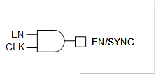
The clock signal can be a logic signal with a logic level as specified in the electrical table, and can be applied directly to the EN/SYNC pin. External logic, such as an AND gate, can be used to combine separate enable and clock inputs, as shown in Figure 6-1.
 Figure 6-1 Synchronization With Separate Enable Signal
(Optional)