SLVSD52A October 2015 – January 2016 TPS63020-Q1
PRODUCTION DATA.
- 1 Features
- 2 Applications
- 3 Description
- 4 Typical Application Schematic
- 5 Revision History
- 6 Device Comparison Table
- 7 Pin Configuration and Functions
- 8 Specifications
- 9 Detailed Description
- 10Application and Implementation
- 11Power Supply Recommendations
- 12Layout
- 13Device and Documentation Support
- 14Mechanical, Packaging, and Orderable Information
Package Options
Mechanical Data (Package|Pins)
- DSJ|14
Thermal pad, mechanical data (Package|Pins)
- DSJ|14
Orderable Information
10 Application and Implementation
NOTE
Information in the following applications sections is not part of the TI component specification, and TI does not warrant its accuracy or completeness. TI’s customers are responsible for determining suitability of components for their purposes. Customers should validate and test their design implementation to confirm system functionality.
10.1 Application Information
The TPS63020-Q1 is a high efficiency, low quiescent current buck-boost converter suitable for applications where the input voltage is higher or lower than the output voltage. Continuous output current can go as high as 2 A in boost mode and as high as 4 A in buck mode. The maximum average current in the switches is limited to a typical value of 4 A.
10.2 Typical Application
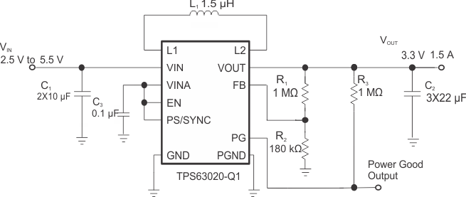 Figure 4. Application Circuit
10.2.1 Design Requirements
The design guidelines provide a component selection to operate the device within the operating conditions specified on the Application Circuit schematic.
Table 1 shows the list of components for the Application Characteristic Curves.
Table 1. List of Components
| REFERENCE | DESCRIPTION | MANUFACTURER |
|---|---|---|
| TPS63020-Q1 | Texas Instruments | |
| L1 | 1.5 μH, 4 mm x 4 mm x 2 mm | XFL4020-152ML, Coilcraft |
| C1 | 2 × 10 μF 6.3V, 0603, X5R ceramic | GRM188R60J106ME84D, Murata |
| C2 | 3 × 22 μF 6.3V, 0603, X5R ceramic | GRM188R60J226MEAOL Murata |
| C3 | 0.1 μF, X5R or X7R ceramic | |
| R1 | Depending on the output voltage at TPS63020 | |
| R2 | Depending on the output voltage at TPS63020 | |
| R3 | 1 MΩ | |
10.2.2 Detailed Design Procedure
The TPS63020-Q1 series of buck-boost converter has internal loop compensation. Therefore, the external L-C filter has to be selected to work with the internal compensation. As a general rule of thumb, the product L x C should not move over a wide range when selecting a different output filter. However, when selecting the output filter a low limit for the inductor value exists to avoid subharmonic oscillation which could be caused by a far too fast ramp up of the amplified inductor current. For the TPS63020-Q1 series the minimum inductor value should be kept at 1 uH.
In particular either 1 µH or 1.5 µH is recommended working at output current between 1.5 A and 2 A. If operating with lower load current is also possible to use 2.2 µH.
Selecting a larger output capacitor value is less critical because the corner frequency moves to lower frequencies.
10.2.2.1 Inductor Selection
For high efficiencies, the inductor should have a low dc resistance to minimize conduction losses. Especially at high-switching frequencies, the core material has a high impact on efficiency. When using small chip inductors, the efficiency is reduced mainly due to higher inductor core losses. This needs to be considered when selecting the appropriate inductor. The inductor value determines the inductor ripple current. The larger the inductor value, the smaller the inductor ripple current and the lower the conduction losses of the converter. Conversely, larger inductor values cause a slower load transient response. To avoid saturation of the inductor, the peak current for the inductor in steady state operation is calculated using Equation 6. Only the equation which defines the switch current in boost mode is shown, because this provides the highest value of current and represents the critical current value for selecting the right inductor.


where
- D =Duty Cycle in Boost mode
- f = Converter switching frequency (typical 2.5MHz)
- L = Inductor value
- η = Estimated converter efficiency (use the number from the efficiency curves or 0.90 as an assumption)
- Note: The calculation must be done for the minimum input voltage possible in boost mode
Calculating the maximum inductor current using the actual operating conditions gives the minimum saturation current of the inductor needed. It's recommended to choose an inductor with a saturation current 20% higher than the value calculated using Equation 2. Possible inductors are listed in Table 2.
Table 2. Inductor Selection(1)
| VENDOR | INDUCTOR SERIES |
|---|---|
| Coilcraft | XFL4020 |
| Toko | FDV0530S |
10.2.2.2 Capacitor Selection
10.2.2.2.1 Input Capacitor
At least a 10 μF input capacitor is recommended to improve transient behavior of the regulator and EMI behavior of the total power supply circuit. A ceramic capacitor placed as close as possible to the VIN and PGND pins of the IC is recommended.
10.2.2.2.2 Output Capacitor
For the output capacitor, use of a small ceramic capacitors placed as close as possible to the VOUT and PGND pins of the IC is recommended. If, for any reason, the application requires the use of large capacitors which can not be placed close to the IC, use a smaller ceramic capacitor in parallel to the large capacitor. The small capacitor should be placed as close as possible to the VOUT and PGND pins of the IC. The recommended typical output capacitor value is 30 µF with a variance that depends on the specific application requirements.
There is also no upper limit for the output capacitance value. Larger capacitors will cause lower output voltage ripple as well as lower output voltage drop during load transients.
When choosing input and output capacitors, it needs to be kept in mind, that the value of capacitance experiences significant losses from their rated value depending on the operating temperature and the operating DC voltage. It is not uncommon for a small surface mount ceramic capacitor to lose 50% and more of its rated capacitance. For this reason it could be important to use a larger value of capacitance or a capacitor with higher voltage rating in order to ensure the required capacitance at the full operating voltage.
10.2.2.2.3 Bypass Capacitor
To make sure that the internal control circuits are supplied with a stable low noise supply voltage, a capacitor can be connected between VINA and GND. Using a ceramic capacitor with a value of 0.1 μF is recommended. The value of this capacitor should not be higher than 0.22 μF.
10.2.2.3 Setting the Output Voltage
The feedback resistor divider must be connected between VOUT, FB and GND. When the output voltage is regulated, the typical value of the voltage at the FB pin is 500 mV. The maximum recommended value for the output voltage is 8 V. The current through the resistive divider should be about 100 times greater than the current into the FB pin. The typical current into the FB pin is 0.01 μA, and the voltage across the resistor between FB and GND, R2, is typically 500 mV. Based on these two values, the recommended value for R2 should be lower than 500 kΩ, in order to set the divider current at 1 μA or higher. It is recommended to keep the value for this resistor in the range of 200 kΩ. From that, the value of the resistor connected between VOUT and FB, R1, depending on the needed output voltage (VOUT), can be calculated using Equation 3:

10.2.3 Application Curves
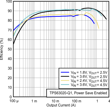
| PS/SYNC = Low | VOUT = 2.5 V, 4.5 V |
Power Save Enabled
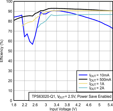
| PS/SYNC = Low | VOUT = 2.5 V |
Power Save Enabled
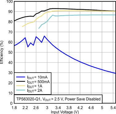
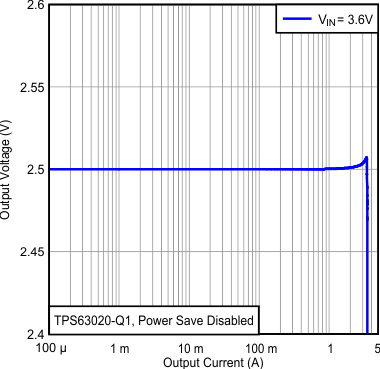
| PS/SYNC = High | VOUT = 2.5 V |
Power Save Disabled
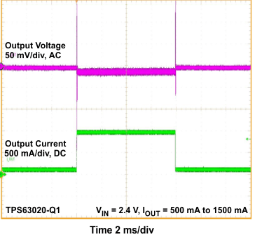
| PS/SYNC = High | VOUT = 3.3 V |
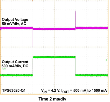
| PS/SYNC = High | VOUT = 3.3 V |
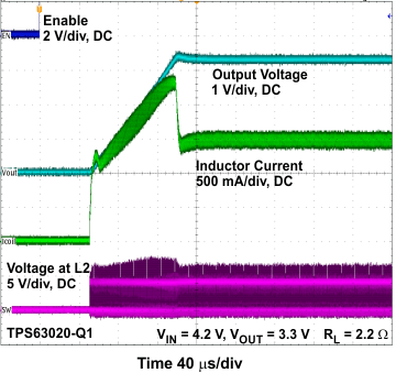
| PS/SYNC = High | VOUT = 3.3 V |
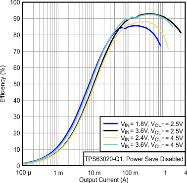
| PS/SYNC = High | VOUT = 2.5 V, 4.5 V |
Power Save Disabled
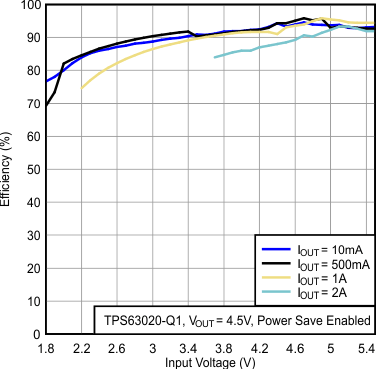
| PS/SYNC = Low | VOUT = 4.5 V |
Power Save Enabled
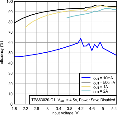
| PS/SYNC = High | VOUT = 4.5 V |
Power Save Disabled
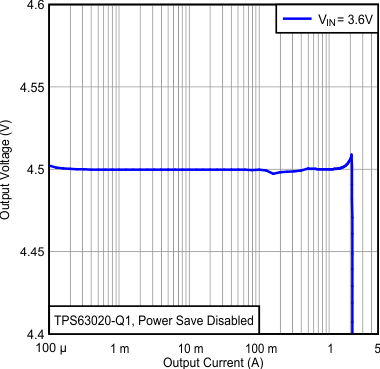
| PS/SYNC = High | VOUT = 4.5 V |
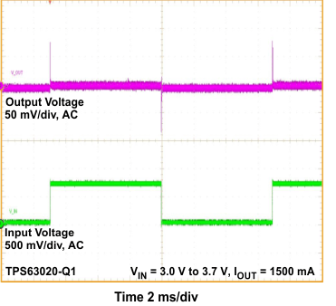
| PS/SYNC = High | VOUT = 3.3 V |
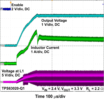
| PS/SYNC = High | VOUT = 3.3 V |
10.3 System Examples
10.3.1 2-A Load Current
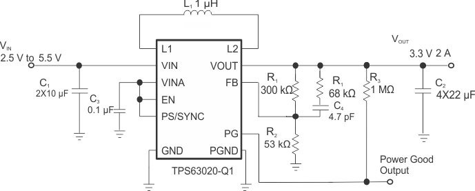 Figure 18. Application Circuit for 2-A Load Current
Capacitor C4 and resistor R1 are added for improved load transient performance.
