SLVSD52A October 2015 – January 2016 TPS63020-Q1
PRODUCTION DATA.
- 1 Features
- 2 Applications
- 3 Description
- 4 Typical Application Schematic
- 5 Revision History
- 6 Device Comparison Table
- 7 Pin Configuration and Functions
- 8 Specifications
- 9 Detailed Description
- 10Application and Implementation
- 11Power Supply Recommendations
- 12Layout
- 13Device and Documentation Support
- 14Mechanical, Packaging, and Orderable Information
Package Options
Mechanical Data (Package|Pins)
- DSJ|14
Thermal pad, mechanical data (Package|Pins)
- DSJ|14
Orderable Information
8 Specifications
8.1 Absolute Maximum Ratings
Over operating junction temperature range (unless otherwise noted)(1)| MIN | MAX | UNIT | ||
|---|---|---|---|---|
| Voltage (2) | VIN, VINA, L1, L2, VOUT, PS/SYNC, EN, FB, PG | –0.3 | 7 | V |
| Operating junction temperature, TJ | –40 | 150 | °C | |
| Storage temperature, Tstg | –65 | 150 | °C | |
(1) Stresses beyond those listed under Absolute Maximum Ratings may cause permanent damage to the device. These are stress ratings only, which do not imply functional operation of the device at these or any other conditions beyond those indicated under Recommended Operating Conditions. Exposure to absolute-maximum-rated conditions for extended periods may affect device reliability.
(2) All voltages are with respect to network ground terminal.
8.2 ESD Ratings
| Value | UNIT | |||
|---|---|---|---|---|
| V(ESD) | Electrostatic discharge(1) | Human body model (HBM), per AEC Q100-002(2) | ±1000 | V |
| Charged device model (CDM), per AEC Q100-011 | ±500 | |||
(1) Electrostatic discharge (ESD) measures device sensitivity and immunity to damage caused by assembly line electrostatic discharges
(2) JAEC Q100-002 indicates HBM stressing is done in accordance with the ANSI/ESDA/JEDEC JS-001 specification
8.3 Recommended Operating Conditions
Over operating junction temperature range (unless otherwise noted)| MIN | NOM | MAX | UNIT | ||
|---|---|---|---|---|---|
| Supply voltage at VIN, VINA | 1.8 | 5.5 | V | ||
| Operating junction temperature range, TJ | –40 | 125 | °C | ||
8.4 Thermal Information
| THERMAL METRIC(1) | TPS63020-Q1 | UNIT | |
|---|---|---|---|
| DSJ (VSON) | |||
| 14 PINS | |||
| RθJA | Junction-to-ambient thermal resistance | 41.8 | °C/W |
| RθJC(top) | Junction-to-case (top) thermal resistance | 47 | °C/W |
| RθJB | Junction-to-board thermal resistance | 17 | °C/W |
| ψJT | Junction-to-top characterization parameter | 0.9 | °C/W |
| ψJB | Junction-to-board characterization parameter | 16.8 | °C/W |
| RθJC(bot) | Junction-to-case (bottom) thermal resistance | 3.6 | °C/W |
(1) For more information about traditional and new thermal metrics, see the Semiconductor and IC Package Thermal Metrics application report, SPRA953.
8.5 Electrical Characteristics
VIN = 1.8 V to 5.5 V, TJ = –40°C to 125°C, typical values are at TA = 25°C (unless otherwise noted)| PARAMETER | TEST CONDITIONS | MIN | TYP | MAX | UNIT | ||
|---|---|---|---|---|---|---|---|
| DC/DC STAGE | |||||||
| VIN | Input voltage range | 1.8 | 5.5 | V | |||
| Minimum input voltage for startup | 0°C ≤ TA ≤ 85°C | 1.5 | 1.8 | 1.9 | V | ||
| Minimum input voltage for startup | 1.5 | 1.8 | 2.0 | V | |||
| VOUT | TPS63020 output voltage range | 1.2 | 5.5 | V | |||
| Duty cycle in step down conversion | 20% | ||||||
| VFB | TPS63020 feedback voltage | PS/SYNC = VIN | 495 | 500 | 505 | mV | |
| VFB | TPS63020 feedback voltage | PS/SYNC = GND referenced to 500 mV | 0.6% | 5% | |||
| Maximum line regulation | 0.5% | ||||||
| Maximum load regulation | 0.5% | ||||||
| f | Oscillator frequency | 2200 | 2400 | 2600 | kHz | ||
| Frequency range for synchronization | 2.0 V ≤ VIN ≤ 5.5 V | 2200 | 2400 | 2600 | kHz | ||
| ISW | Average switch current limit | VIN = VINA = 3.6 V, TJ = 25°C | 3500 | 4000 | 4500 | mA | |
| High side switch on resistance | VIN = VINA = 3.6 V | 50 | mΩ | ||||
| Low side switch on resistance | VIN = VINA = 3.6 V | 50 | mΩ | ||||
| Iq | Quiescent current | VIN and VINA | IO = 0 mA, VEN = VIN = VINA = 3.6 V, VOUT = 3.3 V, -40°C ≤ TJ ≤ 85°C |
25 | 50 | μA | |
| VOUT | 5 | 10 | μA | ||||
| IS | Shutdown current | VEN = 0 V, VIN = VINA = 3.6 V, –40°C ≤ TJ ≤ 85°C | 0.1 | 1 | μA | ||
| CONTROL STAGE | |||||||
| UVLO | Under voltage lockout threshold | VINA voltage decreasing | 1.4 | 1.5 | 1.6 | V | |
| Under voltage lockout hysteresis | 200 | mV | |||||
| VIL | EN, PS/SYNC input low voltage | 0.4 | V | ||||
| VIH | EN, PS/SYNC input high voltage | 1.2 | V | ||||
| EN, PS/SYNC input current | Clamped to GND or VINA | 0.01 | 0.2 | μA | |||
| PG output low voltage | VOUT = 3.3 V, IPGL = 10 μA | 0.04 | 0.4 | V | |||
| PG output leakage current | 0.01 | 0.1 | μA | ||||
| Output overvoltage protection | 5.5 | 7 | V | ||||
| Overtemperature protection | 140 | °C | |||||
| Overtemperature hysteresis | 20 | °C | |||||
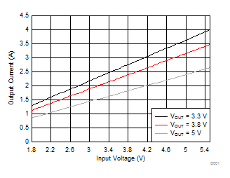
8.6 Typical Characteristics
