SLVSCK8A November   2014  – December 2014 TPS63024 , TPS630241 , TPS630242

PRODUCTION DATA.  

  1. Features
  2. Applications
  3. Description
  4. Revision History
  5. Pin Configuration and Functions
  6. Specifications
    1. 6.1 Absolute Maximum Ratings
    2. 6.2 ESD Ratings
    3. 6.3 Recommended Operating Conditions
    4. 6.4 Thermal Information
    5. 6.5 Electrical Characteristics
    6. 6.6 Timing Requirements
    7. 6.7 Typical Characteristics
  7. Detailed Description
    1. 7.1 Overview
    2. 7.2 Functional Block Diagram
    3. 7.3 Feature Description
      1. 7.3.1 Undervoltage Lockout (UVLO)
      2. 7.3.2 Output Discharge Function
      3. 7.3.3 Thermal Shutdown
      4. 7.3.4 Softstart
      5. 7.3.5 Short Circuit Protection
    4. 7.4 Device Functional Modes
      1. 7.4.1 Control Loop Description
      2. 7.4.2 Power Save Mode Operation
      3. 7.4.3 Current Limit
      4. 7.4.4 Supply and Ground
      5. 7.4.5 Device Enable
  8. Application and Implementation
    1. 8.1 Application Information
    2. 8.2 Typical Application
      1. 8.2.1 Design Requirements
      2. 8.2.2 Detailed Design Procedure
        1. 8.2.2.1 Output Filter Design
        2. 8.2.2.2 Inductor Selection
        3. 8.2.2.3 Capacitor Selection
          1. 8.2.2.3.1 Input Capacitor
          2. 8.2.2.3.2 Output Capacitor
        4. 8.2.2.4 Setting The Output Voltage
      3. 8.2.3 Application Curves
  9. Power Supply Recommendations
  10. 10Layout
    1. 10.1 Layout Guidelines
    2. 10.2 Layout Example
  11. 11Device and Documentation Support
    1. 11.1 Device Support
      1. 11.1.1 Third-Party Products Disclaimer
    2. 11.2 Documentation Support
      1. 11.2.1 Related Documentation
    3. 11.3 Related Links
    4. 11.4 Trademarks
    5. 11.5 Electrostatic Discharge Caution
    6. 11.6 Glossary
  12. 12Mechanical, Packaging, and Orderable Information
  13. 13Mechanical, Packaging, and Orderable Information

Package Options

Mechanical Data (Package|Pins)
Thermal pad, mechanical data (Package|Pins)
Orderable Information

Layout

Layout Guidelines

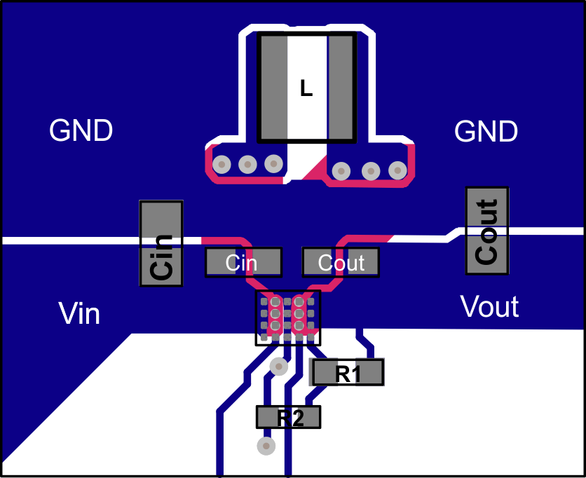
The PCB layout is an important step to maintain the high performance of the TPS63024x devices.

  • Place input and output capacitors as close as possible to the IC. Traces need to be kept short. Routing wide and direct traces to the input and output capacitor results in low trace resistance and low parasitic inductance.
  • Use a common-power GND.
  • The sense trace connected to FB is signal trace. Keep these traces away from L1 and L2 nodes.

Layout Example

TPS63024 TPS630241 TPS630242 PWR553_Layout_suggestion.gif Figure 30. TPS63024x Layout