SLVSCK8A November 2014 – December 2014 TPS63024 , TPS630241 , TPS630242
PRODUCTION DATA.
- 1 Features
- 2 Applications
- 3 Description
- 4 Revision History
- 5 Pin Configuration and Functions
- 6 Specifications
- 7 Detailed Description
- 8 Application and Implementation
- 9 Power Supply Recommendations
- 10Layout
- 11Device and Documentation Support
- 12Mechanical, Packaging, and Orderable Information
- 13Mechanical, Packaging, and Orderable Information
Package Options
Mechanical Data (Package|Pins)
- YFF|20
Thermal pad, mechanical data (Package|Pins)
Orderable Information
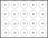
5 Pin Configuration and Functions
WCSP
20-Pin
YFF (TOP VIEW)

Pin Functions
| PIN | I/O | DESCRIPTION | |
|---|---|---|---|
| NAME | NO. | ||
| VOUT | A1,A2,A3 | PWR | Buck-boost converter output |
| FB | A4 | IN | Voltage feedback of adjustable version, must be connected to VOUT for fixed output voltage versions |
| L2 | B1,B2,B3 | PWR | Connection for Inductor |
| PFM/PWM | B4 | IN | set low for PFM mode, set high for forced PWM mode. It must not be left floating |
| PGND | C1,C2,C3 | PWR | Power Ground |
| GND | C4 | PWR | Analog Ground |
| L1 | D1,D2,D3 | PWR | Connection for Inductor |
| EN | D4 | IN | Enable input. Set high to enable and low to disable. It must not be left floating. |
| VIN | E1,E2,E3 | PWR | Supply voltage for power stage |
| VINA | E4 | PWR | Supply voltage for control stage. |