SLVS696D October   2008  – April 2020 TPS63030 , TPS63031

PRODUCTION DATA.  

  1. Features
  2. Applications
  3. Description
    1.     Device Images
      1.      Typical Application Schematic
      2.      Efficiency versus Output Current
  4. Revision History
  5. Output Voltage Options
  6. Pin Configuration and Functions
    1.     Pin Functions
  7. Specifications
    1. 7.1 Absolute Maximum Ratings
    2. 7.2 ESD Ratings
    3. 7.3 Recommended Operating Conditions
    4. 7.4 Thermal Information
    5. 7.5 Electrical Characteristics
    6. 7.6 Typical Characteristics
  8. Detailed Description
    1. 8.1 Overview
    2. 8.2 Functional Block Diagrams
    3. 8.3 Feature Description
      1. 8.3.1 Device Enable
      2. 8.3.2 Undervoltage Lockout
      3. 8.3.3 Overtemperature Protection
    4. 8.4 Device Functional Modes
      1. 8.4.1 Soft Start and Short Circuit Protection
      2. 8.4.2 Buck-Boost Operation
      3. 8.4.3 Power-Save Mode and Synchronization
  9. Application and Implementation
    1. 9.1 Application Information
    2. 9.2 Typical Application
      1. 9.2.1 Design Requirements
      2. 9.2.2 Detailed Design Procedure
        1. 9.2.2.1 Programming the Output Voltage
        2. 9.2.2.2 Inductor Selection
        3. 9.2.2.3 Capacitor Selection
          1. 9.2.2.3.1 Input Capacitor
          2. 9.2.2.3.2 Bypass Capacitor
          3. 9.2.2.3.3 Output Capacitor
      3. 9.2.3 Application Curves
  10. 10Power Supply Recommendations
  11. 11Layout
    1. 11.1 Layout Guidelines
    2. 11.2 Layout Example
    3. 11.3 Thermal Considerations
  12. 12Device and Documentation Support
    1. 12.1 Device Support
      1. 12.1.1 Third-Party Products Disclaimer
    2. 12.2 Documentation Support
      1. 12.2.1 Related Documentation
    3. 12.3 Related Links
    4. 12.4 Support Resources
    5. 12.5 Trademarks
    6. 12.6 Electrostatic Discharge Caution
    7. 12.7 Glossary
  13. 13Mechanical, Packaging, and Orderable Information

Package Options

Mechanical Data (Package|Pins)
Thermal pad, mechanical data (Package|Pins)
Orderable Information

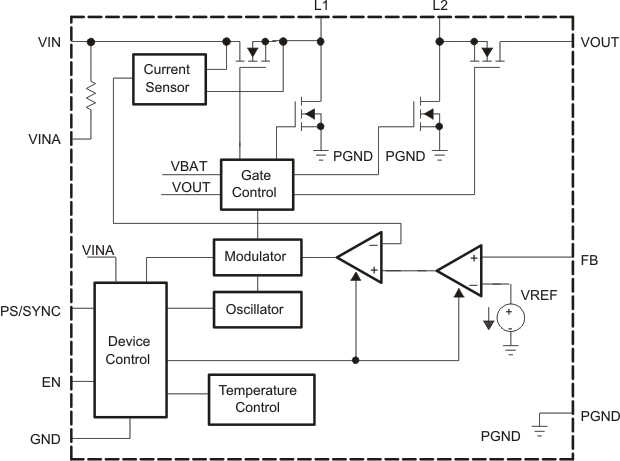
Functional Block Diagrams

TPS63030 TPS63031 fbd_lvs696.gifFigure 3. Functional Block Diagram (TPS63030)
TPS63030 TPS63031 fbdf_lvs696.gifFigure 4. Functional Block Diagram (TPS63031)