SLVSC58B June   2016  – March 2019 TPS63070

PRODUCTION DATA.  

  1. Features
  2. Applications
  3. Description
    1.     Device Images
      1.      Simplified Schematic
      2.      Efficiency vs Output Current; Vo = 5 V
  4. Revision History
  5. Device Comparison Table
  6. Pin Configuration and Functions
    1.     Pin Functions
  7. Specifications
    1. 7.1 Absolute Maximum Ratings
    2. 7.2 ESD Ratings
    3. 7.3 Recommended Operating Conditions
    4. 7.4 Thermal Information
    5. 7.5 Electrical Characteristics
    6. 7.6 Typical Characteristics
  8. Detailed Description
    1. 8.1 Overview
    2. 8.2 Functional Block Diagram TPS63070
    3. 8.3 Functional Block Diagram TPS630701
    4. 8.4 Feature Description
      1. 8.4.1  Control Loop Description
      2. 8.4.2  Precise Enable
      3. 8.4.3  Power Good
      4. 8.4.4  Soft Start
      5. 8.4.5  PS/SYNC
      6. 8.4.6  Short Circuit Protection
      7. 8.4.7  VSEL and FB2 pins
      8. 8.4.8  Overvoltage Protection
      9. 8.4.9  Undervoltage Lockout
      10. 8.4.10 Overtemperature Protection
    5. 8.5 Device Functional Modes
      1. 8.5.1 Power Save Mode
      2. 8.5.2 Current Limit
      3. 8.5.3 Output Discharge Function (TPS630702 only)
  9. Application and Implementation
    1. 9.1 Application Information
    2. 9.2 Typical Application for adjustable version
      1. 9.2.1 Design Requirements
      2. 9.2.2 Detailed Design Procedure
        1. 9.2.2.1 Programming The Output Voltage
        2. 9.2.2.2 Inductor Selection
        3. 9.2.2.3 Capacitor Selection
          1. 9.2.2.3.1 Input Capacitor
          2. 9.2.2.3.2 Output Capacitor
      3. 9.2.3 Application Curves
    3. 9.3 Typical Application for Fixed Voltage Version
      1. 9.3.1 Design Requirements
      2. 9.3.2 Detailed Design Procedure
      3. 9.3.3 Application Curves
  10. 10Power Supply Recommendations
    1. 10.1 Thermal Information
  11. 11Layout
    1. 11.1 Layout Guidelines
    2. 11.2 Layout Example
  12. 12Device and Documentation Support
    1. 12.1 Device Support
      1. 12.1.1 Third-Party Products Disclaimer
    2. 12.2 Related Links
    3. 12.3 Receiving Notification of Documentation Updates
    4. 12.4 Community Resources
    5. 12.5 Trademarks
    6. 12.6 Electrostatic Discharge Caution
    7. 12.7 Glossary
  13. 13Mechanical, Packaging, and Orderable Information

Package Options

Mechanical Data (Package|Pins)
Thermal pad, mechanical data (Package|Pins)
Orderable Information

Application Curves

Table 7. Typical Application Curves for Adjustable Version

Parameter Conditions Figure
Efficiency
Efficiency vs Output Current (PFM/PWM) VIN = 3 V, 4.2 V, 5 V, 7 V, 9 V, 12 V, VOUT = 7 V , PS/SYNC = Low Figure 11
Efficiency vs Output Current (PWM only) VIN = 3 V, 4.2 V, 5 V, 7 V, 9 V, 12 V, VOUT = 7 V , PS/SYNC = High Figure 12
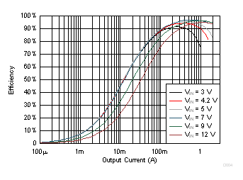
Efficiency vs Output Current (PFM/PWM) VIN = 3 V, 4.2 V, 5 V, 7 V, 9 V, 12 V, VOUT = 9 V , PS/SYNC = Low Figure 13
Efficiency vs Output Current (PWM only) VIN = 3 V, 4.2 V, 5 V, 7 V, 9 V, 12 V, VOUT = 9 V , PS/SYNC = High Figure 14
Load Regulation
Load Regulation, PFM/PWM Operation VIN = 3 V, 4.2 V, 5 V, 7 V, 9 V, 12 V, VOUT = 7 V , PS/SYNC = Low Figure 15
Load Regulation, PWM Operation VIN = 3 V, 4.2 V, 5 V, 7 V, 9 V, 12 V, VOUT = 7 V , PS/SYNC = High Figure 16
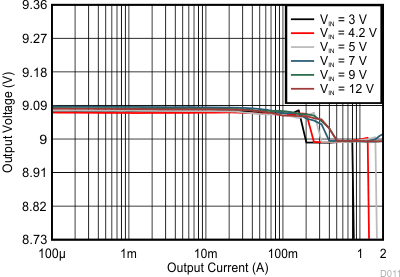
Load Regulation, PFM/PWM Operation VIN = 3 V, 4.2 V, 5 V, 7 V, 9 V, 12 V, VOUT = 9 V , PS/SYNC = Low Figure 17
Load Regulation, PWM Operation VIN = 3 V, 4.2 V, 5 V, 7 V, 9 V, 12 V, VOUT = 9 V , PS/SYNC = High Figure 18
Output Current
Typical Start-up Current vs Input Voltage VOUT = 7 V, TJ = -40 °C, 25 °C, 85 °C, 125 °C Figure 19
Maximum Load Current vs Input Voltage VOUT = 7 V, TJ = -40 °C, 25 °C, 85 °C, 125 °C, PG = high Figure 20
Typical Start-up Current vs Input Voltage VOUT = 9 V, TJ = -40 °C, 25 °C, 85 °C, 125 °C Figure 21
Maximum Load Current vs Input Voltage VOUT = 9V, TJ = -40 °C, 25 °C, 85 °C, 125 °C, PG = high Figure 22
Regulation Accuracy
Load Transient, PFM/PWM Boost Operation VIN = 4.2 V, VOUT = 7 V, Load = 100 mA to 1 A, PS/SYNC = Low Figure 23
Load Transient, PFM/PWM Buck Operation VIN = 12 V, VOUT = 7 V, Load = 200 mA to 1.8 A, PS/SYNC = Low Figure 24
Load Transient, PFM/PWM Boost Operation VIN = 4.2 V, VOUT = 9 V, Load = 100 mA to 1 A, PS/SYNC = Low Figure 25
Load Transient, PFM/PWM Buck Operation VIN = 12 V, VOUT = 9 V, Load = 200 mA to 1.8 A, PS/SYNC = Low Figure 26
Line Transient, PFM/PWM Operation VIN = 5 V to 9 V, VOUT = 7 V, Load = 1 A, PS/SYNC = Low Figure 27
Line Transient, PFM/PWM Operation VIN = 8 V to 12 V, VOUT = 9 V, Load = 1 A, PS/SYNC = Low Figure 28
Output Voltage Ripple
Output Voltage Ripple, PFM/PWM Operation VIN = 5 V, VOUT = 7 V, Load = 0.3 A, PS/SYNC = Low Figure 29
Output Voltage Ripple, PWM Operation VIN = 5 V, VOUT = 7 V, Load = 1 A, PS/SYNC = high Figure 30
Output Voltage Ripple, PFM/PWM Operation VIN = 12 V, VOUT = 7 V, Load = 0.3 A, PS/SYNC = Low Figure 31
Output Voltage Ripple, PFM/PWM Operation VIN = 5 V, VOUT = 9 V, Load = 0.1 A, PS/SYNC = Low Figure 32
Output Voltage Ripple, PWM Operation VIN = 5 V, VOUT = 9 V, Load = 0.5 A, PS/SYNC = high Figure 33
Output Voltage Ripple, PFM/PWM Operation VIN = 12 V, VOUT = 9 V, Load = 0.1 A, PS/SYNC = Low Figure 34
Startup
Start-up Behavior from Rising Enable, PFM/PWM Operation VIN = 4.5 V, VOUT = 7 V, Load = 0.5 A, PS/SYNC = Low Figure 35
Start-up Behavior from Rising Enable, PFM/PWM Operation VIN = 7 V, VOUT = 9 V, Load = 0.5 A, PS/SYNC = Low Figure 36
TPS63070 D003_SLVSC58.gif
Vout = 7 V PFM T = 25 °C
Figure 11. Efficiency vs Output Current
TPS63070 D005_SLVSC58.gif
Vout = 9 V PFM T = 25 °C
Figure 13. Efficiency vs Output Current
TPS63070 D009_SLVSC58.gif
Vout = 7 V PFM T = 25 °C
Figure 15. Output Voltage vs Output Current
TPS63070 D011_SLVSC58.gif
Vout = 9 V PFM T = 25 °C
Figure 17. Output Voltage vs Output Current
TPS63070 D014_SLVSC58.gif
Vout = 7 V resistive load
Figure 19. Typical Start-up Current
TPS63070 D015_SLVSC58.gif
Vout = 9 V resistive load
Figure 21. Typical Start-up Current
TPS63070 Load_Trans_7V_PFM_4V2.gif
Vout = 7 V PFM Vin = 4.2V
Figure 23. Load Transient Response
TPS63070 Load_Trans_9V_VIN4V2.gif
Vout = 9 V PFM Vin = 4.2V
Figure 25. Load Transient Response
TPS63070 Line_Trans_7V.gif
Vout = 7 V PFM Io = 1A
Figure 27. Line Transient Response
TPS63070 37_TPS63070_VOUT_Ripple_7V0_PFM_5V_0p3A.gif
Vin = 5V; Vout = 7 V PFM Io = 0.3A
Figure 29. Output Voltage Ripple
TPS63070 39_TPS63070_VOUT_Ripple_7V0_PFM_12V_0p3A.gif
Vin = 12V; Vout = 7 V PFM Io = 0.3A
Figure 31. Output Voltage Ripple
TPS63070 41_TPS63070_PWM_5Vin_9Vout_500mA.gif
Vin = 5V; Vout = 9 V PWM Io = 0.5A
Figure 33. Output Voltage Ripple
TPS63070 22_TPS63070_startup_timingVIN4V5_Vo5V.gif
Vin = 4.5V; Vout = 7 V PFM Io = 0.5A
Figure 35. Start-up Timing
TPS63070 D004_SLVSC58.gif
Vout = 7 V PWM T = 25 °C
Figure 12. Efficiency vs Output Current
TPS63070 D006_SLVSC58.gif
Vout = 9 V PWM T = 25 °C
Figure 14. Efficiency vs Output Current
TPS63070 D010_SLVSC58.gif
Vout = 7 V PWM T = 25 °C
Figure 16. Output Voltage vs Output Current
TPS63070 D012_SLVSC58.gif
Vout = 9 V PWM T = 25 °C
Figure 18. Output Voltage vs Output Current
TPS63070 D017_SLVSC58.gif
Vout = 7 V after start-up with PG = high
Figure 20. Maximum Load Current vs Input Voltage
TPS63070 D018_SLVSC58.gif
Vout = 9 V after start-up with PG = high
Figure 22. Maximum Load Current vs Input Voltage
TPS63070 Load_Trans_7V_PFM_12V.gif
Vout = 7 V PFM Vin = 12V
Figure 24. Load Transient Response
TPS63070 Load_Trans_9V_VIN12V.gif
Vout = 9 V PFM Vin = 12V
Figure 26. Load Transient Response
TPS63070 Line_Trans_9V.gif
Vout = 9 V PFM Io = 1A
Figure 28. Line Transient Response
TPS63070 38_TPS63070_VOUT_Ripple_7V0_PWM_5V_1A.gif
Vin = 5V; Vout = 7 V PWM Io = 1A
Figure 30. Output Voltage Ripple
TPS63070 40_TPS63070_PFM_5Vin_9Vout_100mA.gif
Vin = 5V; Vout = 9 V PFM Io = 0.1A
Figure 32. Output Voltage Ripple
TPS63070 42_TPS63070_PFM_12Vin_9Vout_100mA.gif
Vin = 12V; Vout = 9 V PFM Io = 0.1A
Figure 34. Output Voltage Ripple
TPS63070 32_TPS63070_startup_timingVIN7V_Vo9V.gif
Vin = 7V; Vout = 9 V PFM Io = 0.5A
Figure 36. Start-up Timing