SLVSFH3B October 2021 – June 2022 TPS631000
PRODUCTION DATA
- 1 Features
- 2 Applications
- 3 Description
- 4 Revision History
- 5 Pin Configuration and Functions
- 6 Specifications
- 7 Detailed Description
- 8 Application and Implementation
- 9 Power Supply Recommendations
- 10Layout
- 11Device and Documentation Support
- 12Mechanical, Packaging, and Orderable Information
Package Options
Mechanical Data (Package|Pins)
- DRL|8
Thermal pad, mechanical data (Package|Pins)
Orderable Information
8.2.2.2 Inductor Selection
The inductor selection is affected by several parameters such as the following:
- Inductor ripple current
- Output voltage ripple
- Transition point into power save mode
- Efficiency
See Table 8-2 for typical inductors.
For high efficiencies, the inductor should have a low DC resistance to minimize conduction losses. Especially at high-switching frequencies, the core material has a high impact on efficiency. When using small chip inductors, the efficiency is reduced mainly due to higher inductor core losses. This needs to be considered when selecting the appropriate inductor. The inductor value determines the inductor ripple current. The larger the inductor value, the smaller the inductor ripple current and the lower the conduction losses of the converter. Conversely, larger inductor values cause a slower load transient response. To avoid saturation of the inductor, the peak current for the inductor in steady state operation is calculated using Equation 3. Only the equation that defines the switch current in boost mode is shown because this provides the highest value of current and represents the critical current value for selecting the right inductor.
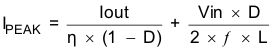
where:
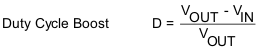
- D = duty cycle in boost mode
- f = converter switching frequency (typical 2.2 MHz)
- L = inductor value
- η = estimated converter efficiency (use the number from the efficiency curves or 0.9 as an assumption)
The calculation must be done for the minimum input voltage in boost mode.
Calculating the maximum inductor current using the actual operating conditions gives the minimum saturation current of the inductor needed. It is recommended to choose an inductor with a saturation current 20% higher than the value calculated using Equation 3. Possible inductors are listed in Table 8-2.
| INDUCTOR VALUE [µH] | SATURATION CURRENT [A] | DCR [mΩ] | PART NUMBER | MANUFACTURER(1) | SIZE (L × W × H mm) |
|---|---|---|---|---|---|
| 1 | 4.3 | 42 | DFE252012P-1R0M=P2 | MuRata | 2.5 × 2.0 × 1.2 |
| 1 | 4.2 | 43 | HTEK20161T-1R0MSR | Cyntec | 2.0 × 1.6 × 1.0 |
| 1 | 2.2 | 75 | MAKK2016T1R0M (2) | Taiyo Yuden | 2.0 × 1.6 × 1.0 |
| 1 | 2.0 | 144 | DFE18SAN1R0ME0 (2) | Murata | 1.6 × 0.8 × 0.8 |