SLVSFH3B October   2021  – June 2022 TPS631000

PRODUCTION DATA  

  1. Features
  2. Applications
  3. Description
  4. Revision History
  5. Pin Configuration and Functions
  6. Specifications
    1. 6.1 Absolute Maximum Ratings
    2. 6.2 ESD Rating
    3. 6.3 Recommended Operating Conditions
    4. 6.4 Thermal Information
    5. 6.5 Electrical Characteristics 
  7. Detailed Description
    1. 7.1 Overview
    2. 7.2 Functional Block Diagram
    3. 7.3 Feature Description
      1. 7.3.1 Undervoltage Lockout (UVLO)
      2. 7.3.2 Enable and Soft Start
      3. 7.3.3 Adjustable Output Voltage
      4. 7.3.4 Mode Selection (PFM/FPWM)
      5. 7.3.5 Reverse Current Operation
      6. 7.3.6 Protection Features
        1. 7.3.6.1 Input Overvoltage Protection
        2. 7.3.6.2 Output Overvoltage Protection
        3. 7.3.6.3 Short Circuit Protection
        4. 7.3.6.4 Thermal Shutdown
    4. 7.4 Device Functional Modes
  8. Application and Implementation
    1. 8.1 Application Information
    2. 8.2 Typical Application
      1. 8.2.1 Design Requirements
      2. 8.2.2 Detailed Design Procedure
        1. 8.2.2.1 Custom Design with WEBENCH Tools
        2. 8.2.2.2 Inductor Selection
        3. 8.2.2.3 Output Capacitor Selection
        4. 8.2.2.4 Input Capacitor Selection
        5. 8.2.2.5 Setting the Output Voltage
      3. 8.2.3 Application Curves
  9. Power Supply Recommendations
  10. 10Layout
    1. 10.1 Layout Guidelines
    2. 10.2 Layout Example
  11. 11Device and Documentation Support
    1. 11.1 Device Support
      1. 11.1.1 Third-Party Products Disclaimer
      2. 11.1.2 Development Support
        1. 11.1.2.1 Custom Design with WEBENCH Tools
    2. 11.2 Receiving Notification of Documentation Updates
    3. 11.3 Support Resources
    4. 11.4 Trademarks
    5. 11.5 Electrostatic Discharge Caution
    6. 11.6 Glossary
  12. 12Mechanical, Packaging, and Orderable Information

Package Options

Mechanical Data (Package|Pins)
Thermal pad, mechanical data (Package|Pins)
Orderable Information

Description

The TPS631000 is a constant frequency peak current mode control buck-boost converter. The device has a 3-A peak current limit (typical) and 1.6-V to 5.5-V input voltage range. The TPS631000 provides a power supply solution for system pre-regulators and voltage stabilizers.

Depending on the input voltage, the TPS631000 automatically operates in boost, buck, or in 3-cycle buck-boost mode when the input voltage is approximately equal to the output voltage. The transitions between modes happen at a defined duty cycle and avoid unwanted toggling within the modes to reduce output voltage ripple. 8-μA quiescent current and power save mode power enable the highest efficiency for light to no-load conditions.

The TPS631000 offers a very small solution size with a 1.2-mm × 2.1-mm SOT-583 package, a 1-μH inductor, and one 0805 output capacitor.

Device Information
PART NUMBERPACKAGE(1)BODY SIZE (NOM)
TPS631000SOT-5831.6 mm × 2.1 mm
For all available packages, see the orderable addendum at the end of the data sheet.
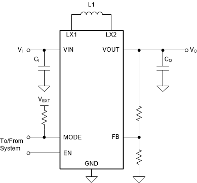
GUID-ADE92E27-7F16-442F-B448-EBC19B4EC24A-low.gifTypical Application
Efficiency Target vs Output Current (VOUT = 3.3 V)