SLVSFH3B October   2021  – June 2022 TPS631000

PRODUCTION DATA  

  1. Features
  2. Applications
  3. Description
  4. Revision History
  5. Pin Configuration and Functions
  6. Specifications
    1. 6.1 Absolute Maximum Ratings
    2. 6.2 ESD Rating
    3. 6.3 Recommended Operating Conditions
    4. 6.4 Thermal Information
    5. 6.5 Electrical Characteristics 
  7. Detailed Description
    1. 7.1 Overview
    2. 7.2 Functional Block Diagram
    3. 7.3 Feature Description
      1. 7.3.1 Undervoltage Lockout (UVLO)
      2. 7.3.2 Enable and Soft Start
      3. 7.3.3 Adjustable Output Voltage
      4. 7.3.4 Mode Selection (PFM/FPWM)
      5. 7.3.5 Reverse Current Operation
      6. 7.3.6 Protection Features
        1. 7.3.6.1 Input Overvoltage Protection
        2. 7.3.6.2 Output Overvoltage Protection
        3. 7.3.6.3 Short Circuit Protection
        4. 7.3.6.4 Thermal Shutdown
    4. 7.4 Device Functional Modes
  8. Application and Implementation
    1. 8.1 Application Information
    2. 8.2 Typical Application
      1. 8.2.1 Design Requirements
      2. 8.2.2 Detailed Design Procedure
        1. 8.2.2.1 Custom Design with WEBENCH Tools
        2. 8.2.2.2 Inductor Selection
        3. 8.2.2.3 Output Capacitor Selection
        4. 8.2.2.4 Input Capacitor Selection
        5. 8.2.2.5 Setting the Output Voltage
      3. 8.2.3 Application Curves
  9. Power Supply Recommendations
  10. 10Layout
    1. 10.1 Layout Guidelines
    2. 10.2 Layout Example
  11. 11Device and Documentation Support
    1. 11.1 Device Support
      1. 11.1.1 Third-Party Products Disclaimer
      2. 11.1.2 Development Support
        1. 11.1.2.1 Custom Design with WEBENCH Tools
    2. 11.2 Receiving Notification of Documentation Updates
    3. 11.3 Support Resources
    4. 11.4 Trademarks
    5. 11.5 Electrostatic Discharge Caution
    6. 11.6 Glossary
  12. 12Mechanical, Packaging, and Orderable Information

Package Options

Mechanical Data (Package|Pins)
Thermal pad, mechanical data (Package|Pins)
Orderable Information

Device Functional Modes

The device has two functional modes: off and on. The device enters the on mode when the voltage on the VIN pin is higher than the UVLO threshold and a high logic level is applied to the EN pin. The device enters the off mode when the voltage on the VIN pin is lower than the UVLO threshold or a low logic level is applied to the EN pin.
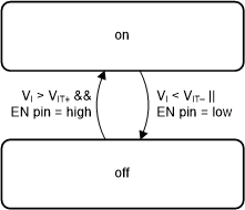
GUID-2945CACB-D8EC-4D9E-8409-EF1424DB3188-low.gifFigure 7-3 Device Functional Modes