SLVSH51 july 2023 TPS631012 , TPS631013
PRODMIX
- 1
- 1 Features
- 2 Applications
- 3 Description
- 4 Revision History
- 5 Device Comparison Table
- 6 Pin Configuration and Functions
- 7 Specifications
-
8 Detailed Description
- 8.1 Overview
- 8.2 Functional Block Diagram
- 8.3 Feature Description
- 8.4 Device Functional Modes
- 8.5 Programming
- 8.6 Register Map
- 9 Application and Implementation
- 10Device and Documentation Support
- 11Mechanical, Packaging, and Orderable Information
Package Options
Mechanical Data (Package|Pins)
- YBG|8
Thermal pad, mechanical data (Package|Pins)
Orderable Information
8.3.2 Enable and Soft Start
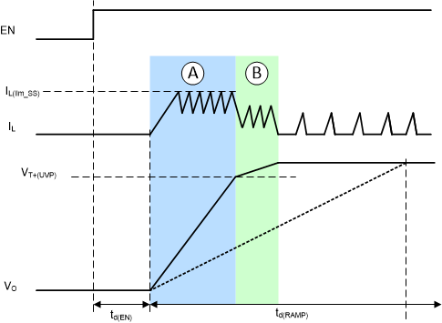
 Figure 8-1 Typical Soft-Start
Behavior
Figure 8-1 Typical Soft-Start
BehaviorWhen the input voltage is above the UVLO rising threshold and the EN pin is pulled to a voltage above 1.2 V, the TPS631012 and TPS631013 are enabled and start up after a short delay time, td(EN).
The TPS631012 and TPS631013 have two start-up mechanisms that are controlled by the FAST_RAMP_EN bit in Register CONTROL2. Figure 8-1 shows a typical start-up case (low output load, typical output capacitance).
- When FAST_RAMP_EN = 1, the fast ramp mode is enabled. The output ramp behavior is shown as the solid line Vo in Figure 8-1
- When FAST_RAMP_EN = 0, the fast ramp mode is disabled. The output ramp behavior is shown as the dash line Vo in Figure 8-1
When fast ramp mode is enabled, the devices control the inductor peak current to limit the inrush current and ensure the fastest possible soft start if the capacitance is chosen lower than that for which the ramp time td(RAMP) was selected. The output voltage then rises faster than the reference voltage ramp (see phase A in Figure 8-1). To avoid an output overshoot, the current clamp is deactivated when the output is close to the target voltage and follows the reference voltage ramp slew value given by the voltage ramp, which is finishing the start up (see phase B in Figure 8-1). Transition from the current clamp operation is detected using the VT+(UVP) threshold, which is typically 90% of the target output voltage. After phase B, the output voltage is well regulated to the nominal target voltage. The current waveform depends on the output load and operation mode. The current limit during start-up has two options and is controlled by the CL_RAMP_MIN bit in Register CONTROL2.
- When CL_RAMP_MIN = 0, the typical current limit during start-up (phase A in Figure 8-1) is 500mA
- When CL_RAMP_MIN = 1, the typical current limit during start-up (phase A in Figure 8-1) is 1000mA
When fast ramp mode is disabled, the output voltage is totally controlled by the internal reference voltage ramp slew rate. There are three bits of TD_RAMP in Register CONTROL2 to define the output voltage ramp time.
Note that if, during start-up, the current limit (IL(lim_SS)) is lower than the current required to follow the voltage ramp controlled by TD_RAMP, the current automatically increases to follow the voltage ramp.