SLVSEU9D November 2018 – January 2021 TPS63802
PRODUCTION DATA
- 1 Features
- 2 Applications
- 3 Description
- 4 Revision History
- 5 Description (continued)
- 6 Device Comparison Table
- 7 Pin Configuration and Functions
- 8 Specifications
-
9 Detailed Description
- 9.1 Overview
- 9.2 Functional Block Diagram
- 9.3
Feature Description
- 9.3.1 Control Loop Description
- 9.3.2 Precise Device Enable: Threshold- or Delayed Enable
- 9.3.3 Mode Selection (PFM/PWM)
- 9.3.4 Undervoltage Lockout (UVLO)
- 9.3.5 Soft Start
- 9.3.6 Adjustable Output Voltage
- 9.3.7 Overtemperature Protection - Thermal Shutdown
- 9.3.8 Input Overvoltage - Reverse-Boost Protection (IVP)
- 9.3.9 Output Overvoltage Protection (OVP)
- 9.3.10 Power-Good Indicator
- 9.4 Device Functional Modes
- 10Application and Implementation
- 11Power Supply Recommendations
- 12Layout
- 13Device and Documentation Support
- 14Mechanical, Packaging, and Orderable Information
Package Options
Mechanical Data (Package|Pins)
- DLA|10
Thermal pad, mechanical data (Package|Pins)
Orderable Information
9.4.2 Power Save Mode Operation
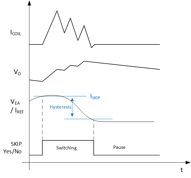
Besides continuos conduction mode (PWM), the TPS63802 features power safe mode (PFM) operation to achieve high efficiency at light load currents. This is implemented by pausing the switching operation, depending on the load current.
The skip comparator manages the switching or pause operation. It compares the current demand signal from the voltage loop, IREF, with the skip threshold, ISKIP, as shown in Figure 9-1. If the current demand is lower than the skip value, the comparator pauses switching operation. If the current demand goes higher (due to falling VO), the comparator activates the current loop and allows switching according to the loop behavior. Whenever the current loop has risen VO by bringing charge to the output, the voltage loop output, IREF (respectively VEA), decreases. When IREF falls below ISKIP-hysteresis, it automatically pauses again.
 Figure 9-10 Power Safe Mode Operation Curves