SLVSDS9E July 2018 – August 2021 TPS63805 , TPS63806 , TPS63807
PRODUCTION DATA
- 1 Features
- 2 Applications
- 3 Description
- 4 Revision History
- 5 Description (continued)
- 6 Device Comparison Table
- 7 Pin Configuration and Functions
- 8 Specifications
-
9 Detailed Description
- 9.1 Overview
- 9.2 Functional Block Diagram
- 9.3
Feature Description
- 9.3.1 Control Loop Description
- 9.3.2 Precise Device Enable: Threshold- or Delayed Enable
- 9.3.3 Mode Selection (PFM/PWM)
- 9.3.4 Undervoltage Lockout (UVLO)
- 9.3.5 Soft Start
- 9.3.6 Adjustable Output Voltage
- 9.3.7 Overtemperature Protection - Thermal Shutdown
- 9.3.8 Input Overvoltage - Reverse-Boost Protection (IVP)
- 9.3.9 Output Overvoltage Protection (OVP)
- 9.3.10 Power-Good Indicator
- 9.4 Device Functional Modes
- 10Application and Implementation
- 11Power Supply Recommendations
- 12Layout
- 13Device and Documentation Support
- 14Mechanical, Packaging, and Orderable Information
Package Options
Mechanical Data (Package|Pins)
- YFF|15
Thermal pad, mechanical data (Package|Pins)
Orderable Information
9.4.1.3 Buck-Boost Operation
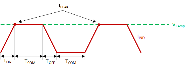
When VI is close to VO, the TPS63805, TPS63806, and TPS63807 operate in buck-boost mode where all switches are active and the device repeats 3-cycles:
- TON: Boost-charge phase where boost low-side and buck high-side are closed and the inductor current is built up
- TOFF: Buck discharge phase where boost high-side and buck low-side are closed and the inductor is discharged
- TCOM: VI connected to VO where all high-side switches are closed and the input is connected to the output
 Figure 9-8 Peak-Current Buck-Boost Operation