SLVSEK4C July   2019  – February 2020 TPS63810 , TPS63811

PRODUCTION DATA.  

  1. Features
  2. Applications
  3. Description
    1.     Device Images
      1.      Simplified Schematic
      2.      Efficiency versus Output Current
  4. Revision History
  5. Device Comparison Table
  6. Pin Configuration and Functions
    1.     BGA Package (YFF) Pin Functions
  7. Specifications
    1. 7.1 Absolute Maximum Ratings
    2. 7.2 ESD Ratings
    3. 7.3 Recommended Operating Conditions
    4. 7.4 Thermal Information
    5. 7.5 Electrical Characteristics
    6. 7.6 Timing Requirements
    7. 7.7 Switching Characteristics
    8. 7.8 Typical Characteristics
  8. Detailed Description
    1. 8.1 Overview
    2. 8.2 Functional Block Diagram
    3. 8.3 Feature Description
      1. 8.3.1  Control Scheme
        1. 8.3.1.1 Buck Operation
        2. 8.3.1.2 Boost Operation
        3. 8.3.1.3 Buck-Boost Operation
      2. 8.3.2  Control Scheme
      3. 8.3.3  Power-Save Mode Operation (PSM)
      4. 8.3.4  Forced-PWM Operation (FPWM)
      5. 8.3.5  Ramp-PWM Operation (RPWM)
      6. 8.3.6  Device Enable (EN)
      7. 8.3.7  Undervoltage Lockout (UVLO)
      8. 8.3.8  Soft Start
      9. 8.3.9  Output Voltage Control
        1. 8.3.9.1 Dynamic Voltage Scaling
      10. 8.3.10 Protection Functions
        1. 8.3.10.1 Input Voltage Protection (IVP)
        2. 8.3.10.2 Current Limit Mode and Overcurrent Protection
        3. 8.3.10.3 Thermal Shutdown
      11. 8.3.11 Power Good
      12. 8.3.12 Load Disconnect
      13. 8.3.13 Output Discharge
    4. 8.4 Device Functional Modes
    5. 8.5 Programming
      1. 8.5.1 Serial Interface Description
      2. 8.5.2 Standard-, Fast-, and Fast-Mode Plus Protocol
      3. 8.5.3 I2C Update Sequence
    6. 8.6 Register Map
      1. 8.6.1 Register Description
        1. 8.6.1.1 Register Map
        2. 8.6.1.2 Register CONTROL (Slave address: 0b1110101; Register address: 0x01; Default: 0x00 or 0x20)
          1. Table 3. Register CONTROL Field Descriptions
        3. 8.6.1.3 Register STATUS (Slave address: 0b1110101; Register address: 0x02; Default: 0x00)
          1. Table 4. Register STATUS Field Descriptions
        4. 8.6.1.4 Register DEVID (Slave address: 0b1110101; Register address: 0x03; Default: 0x04)
          1. Table 5. Register DEVID Field Descriptions
        5. 8.6.1.5 Register VOUT1 (Slave address: 0b1110101; Register address: 0x04; Default: 0x3C)
          1. Table 6. Register VOUT1 Field Descriptions
        6. 8.6.1.6 Register VOUT2 (Slave address: 0b1110101; Register address: 0x05; Default: 0x42)
          1. Table 7. Register VOUT2 Field Descriptions
  9. Application and Implementation
    1. 9.1 Application Information
    2. 9.2 Typical Applications
      1. 9.2.1 1.8-V to 5.2-V Output Smartphone Power Supply
        1. 9.2.1.1 Design Requirements
        2. 9.2.1.2 Detailed Design Procedure
          1. 9.2.1.2.1 Input Capacitor Selection
          2. 9.2.1.2.2 Inductor Selection
          3. 9.2.1.2.3 Output Capacitor Selection
          4. 9.2.1.2.4 I2C Pullup Resistor Selection
        3. 9.2.1.3 Application Curves
  10. 10Power Supply Recommendations
  11. 11Layout
    1. 11.1 Layout Guidelines
    2. 11.2 Layout Example
  12. 12Device and Documentation Support
    1. 12.1 Device Support
      1. 12.1.1 Third-Party Products Disclaimer
    2. 12.2 Documentation Support
      1. 12.2.1 Related Documentation
    3. 12.3 Related Links
    4. 12.4 Receiving Notification of Documentation Updates
    5. 12.5 Support Resources
    6. 12.6 Trademarks
    7. 12.7 Glossary
  13. 13Mechanical, Packaging, and Orderable Information

Package Options

Mechanical Data (Package|Pins)
Thermal pad, mechanical data (Package|Pins)
Orderable Information

Application Curves

Table 10 lists the components that were used for the measurements contained in the following pages.

Table 10. Components for Application Characteristic Curves

REFERENCE DESCRIPTION PART NUMBER MANUFACTURER
C1 Capacitor, 10 µF, 10 V, 0603, ceramic GRM188R61A106ME69 Murata
C2, C3 Capacitor, 22 µF, 10 V, 0603, ceramic GRM187R61A226ME15 Murata
L1 Inductor, 0.47 µH XFL4015-471MEC Coilcraft
U1 Integrated circuit TPS63810YFF Texas Instruments

WHITESPACE

TPS63810 TPS63811 D001-SLVSEK4-01.gif
VI = 3.6 V PSM TA = 25°C
Figure 32. Efficiency versus Output Current
TPS63810 TPS63811 D014-SLVSEK4-01.gif
VI = 3.6 V FPWM TA = 25°C
Figure 34. Load Regulation
TPS63810 TPS63811 scope-06-slvsek4.gif
VI = 5 V PSM TA = 25°C
VO = 3.3 V IO = 100 mA
Figure 36. PFM Switching Waveforms
(Buck Operation)
TPS63810 TPS63811 scope-08-slvsek4.gif
VI = 2.5 V PSM TA = 25°C
VO = 3.3 V IO = 100 mA
Figure 38. PFM Switching Waveforms
(Boost Operation)
TPS63810 TPS63811 scope-05-slvsek4.gif
VI = 3.3 V FPWM TA = 25°C
VO = 3.3 V IO = 100 mA
Figure 40. PWM Switching Waveforms
(Buck-Boost Operation)
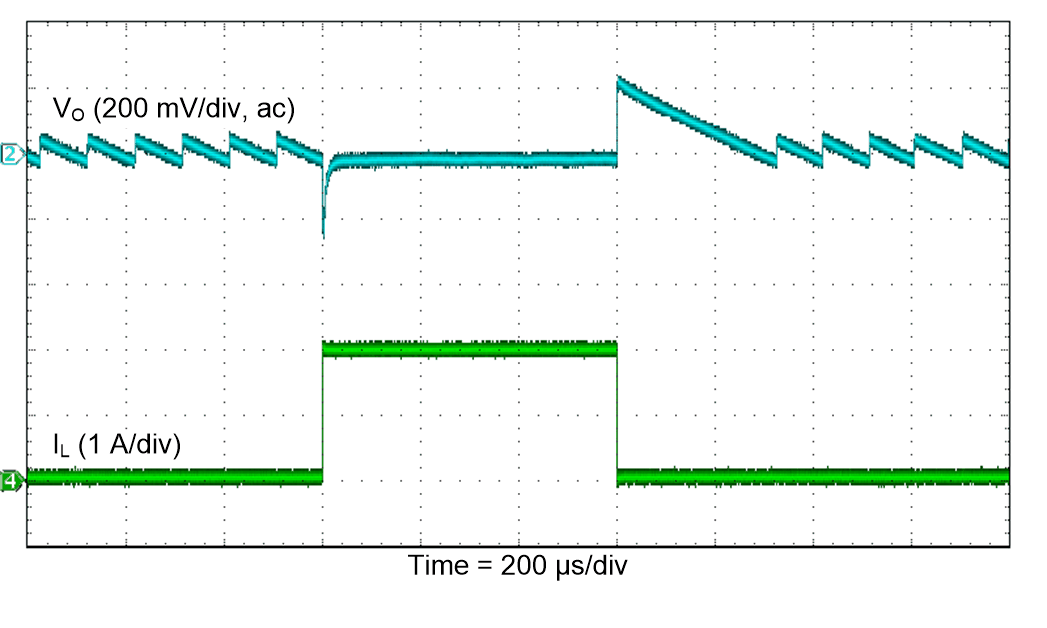
TPS63810 TPS63811 scope-02-slvsek4.gif
VI = 2.5 V to 5.5 V PSM TA = 25°C
VO = 3.3 V IO = 200 mA
Figure 42. Line Transient Response
TPS63810 TPS63811 scope-15-slvsek4.gif
VI = 4.2 V PSM TA = 25°C
VO = 3.3 V IO = 10 mA to 2 A
Figure 44. Load Transient Response (Buck)
TPS63810 TPS63811 scope-17-slvsek4.gif
VI = 2.6 V PSM TA = 25°C
VO = 3.3 V IO = 10 mA to 2 A
Figure 46. Load Transient Response (Boost)
TPS63810 TPS63811 scope-09-slvsek4.gif
VI = 3.6 V PSM TA = 25°C
VO = 3.3 V RL = 33 Ω
Figure 48. Start-Up Waveforms
(Light Load)
TPS63810 TPS63811 scope-11-slvsek4.gif
VI = 3.6 V PSM TA = 25°C
VO = 2 V to 4 V RL = 330 Ω
Figure 50. Dynamic Voltage Scaling (PFM)
TPS63810 TPS63811 scope-18-slvsek4.gif
VI = 3.6 V PSM TA = 25°C
VO = 3.3 V
Figure 52. Overcurrent Protection
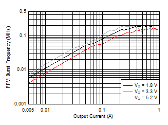
TPS63810 TPS63811 D016-SLVSEK4-01.gif
VI = 3.6 V PSM TA = 25°C
Figure 54. Burst Switching Frequency versus Output Current
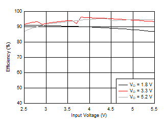
TPS63810 TPS63811 D002-SLVSEK4-01.gif
IO = 1 A PSM TA = 25°C
Figure 33. Efficiency versus Input Voltage
TPS63810 TPS63811 D015-SLVSEK4-02.gif
IO = 1 A FPWM TA = 25°C
Figure 35. Line Regulation
TPS63810 TPS63811 scope-07-slvsek4.gif
VI = 3.3 V PSM TA = 25°C
VO = 3.3 V IO = 100 mA
Figure 37. PFM Switching Waveforms
(Buck-Boost Operation)
TPS63810 TPS63811 scope-test-slvsek4.gif
VI = 5 V FPWM TA = 25°C
VO = 3.3 V IO = 100 mA
Figure 39. PWM Switching Waveforms
(Buck Operation)
TPS63810 TPS63811 scope-04-slvsek4.gif
VI = 2.5 V FPWM TA = 25°C
VO = 3.3 V IO = 100 mA
Figure 41. PWM Switching Waveforms
(Boost Operation)
TPS63810 TPS63811 scope-01-slvsek4.gif
VI = 2.5 V to 5.5 V PSM TA = 25°C
VO = 3.3 V IO = 2 A
Figure 43. Line Transient Response
TPS63810 TPS63811 scope-16-slvsek4.gif
VI = 3.3 V PSM TA = 25°C
VO = 3.3 V IO = 10 mA to 2 A
Figure 45. Load Transient Response (Buck-Boost)
TPS63810 TPS63811 scope-14-slvsek4.gif
VI = 3.3 V ±0.9 V FPWM TA = 25°C
VO = 3.3 V RL = 3 Ω
Figure 47. Line Sweep (PWM)
TPS63810 TPS63811 scope-10-slvsek4.gif
VI = 3.6 V PSM TA = 25°C
VO = 3.3 V RL = 3.3 Ω
Figure 49. Start-Up Waveforms
(Heavy Load)
TPS63810 TPS63811 scope-12-slvsek4.gif
VI = 3.6 V PSM TA = 25°C
VO = 2 V to 4 V RPWM RL = 330 Ω
Figure 51. Dynamic Voltage Scaling (RPWM)
TPS63810 TPS63811 D009-SLVSEK4-01.gif
IO = 1 A FPWM TA = 25°C
VI rising
Figure 53. Switching Frequency versus Input Voltage
TPS63810 TPS63811 D013-SLVSEK4-01.gif
PSM TA = 25°C
Figure 55. Maximum Output Current versus Input Voltage