SLVSGC1B December 2021 – August 2024 TPS63901
PRODUCTION DATA
- 1
- 1 Features
- 2 Applications
- 3 Description
- 4 Pin Configuration and Functions
- 5 Specifications
-
6 Detailed Description
- 6.1 Overview
- 6.2 Functional Block Diagram
- 6.3 Feature Description
- 6.4 Device Functional Modes
- 7 Application and Implementation
- 8 Power Supply Recommendations
- 9 Layout
- 10Device and Documentation Support
- 11Revision History
- 12Mechanical, Packaging, and Orderable Information
Package Options
Refer to the PDF data sheet for device specific package drawings
Mechanical Data (Package|Pins)
- YCJ|12
Thermal pad, mechanical data (Package|Pins)
Orderable Information
3 Description
The TPS63901 device is a high-efficiency synchronous buck-boost converter with an extremely low quiescent current (75 nA typical). The device has 32 user-programmable output voltage settings from 1.8 V to 5 V.
A dynamic voltage-scaling feature lets applications switch between two output voltages during operation; for example, to save power by using a lower system supply voltage during standby operation.
With its wide supply voltage range and programmable input current limit (1 mA to 100 mA and unlimited), the device is ideal for use with a wide range of primary like 3S Alkaline, 1S Li-MnO2 or 1S Li-SOCl2, and secondary battery types.
The high-output current capability supports commonly-used RF standards like sub-1-GHz, BLE, LoRa, wM-Bus, and NB-IoT.
| Part Number(1) | Package | Body Size (NOM) |
|---|---|---|
| TPS63901 | WCSP (12) | 1.50 mm × 1.15 mm |
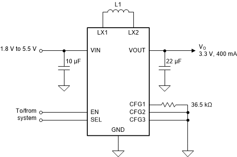
 Simplified Schematic