SLVSC45C August 2013 – June 2017 TPS65000-Q1
PRODUCTION DATA.
- 1 Features
- 2 Applications
- 3 Description
- 4 Revision History
- 5 Pin Configuration and Functions
- 6 Specifications
- 7 Detailed Description
- 8 Application and Implementation
- 9 Power Supply Recommendations
- 10Layout
- 11Device and Documentation Support
- 12Mechanical, Packaging, and Orderable Information
Package Options
Mechanical Data (Package|Pins)
- RTE|16
Thermal pad, mechanical data (Package|Pins)
- RTE|16
Orderable Information
6 Specifications
6.1 Absolute Maximum Ratings
over operating free-air temperature range (unless otherwise noted)(1)
(1) Stresses beyond those listed under Absolute Maximum Ratings may cause permanent damage to the device. These are stress ratings only, and functional operation of the device at these or any other conditions beyond those indicated under Recommended Operating Conditions is not implied. Exposure to absolute-maximum-rated conditions for extended periods may affect device reliability.
6.2 ESD Ratings
| VALUE | UNIT | |||||
|---|---|---|---|---|---|---|
| V(ESD) | Electrostatic discharge | Human body model (HBM), per AEC Q100-002(1) | ±2500 | V | ||
| Charged device model (CDM), per AEC Q100-011 | Corner pins (1, 4, 5, 8, 9, 12, 13, and 16) | ±750 | ||||
| Other pins | ±500 | |||||
(1) AEC Q100-002 indicates HBM stressing is done in accordance with the ANSI/ESDA/JEDEC JS-001 specification.
6.3 Recommended Operating Conditions
6.4 Thermal Information
| THERMAL METRIC(1) | TPS65000-Q1 | UNIT | |
|---|---|---|---|
| RTE (WQFN) | |||
| 16 PINS | |||
| RθJA | Junction-to-ambient thermal resistance | 46.4 | °C/W |
| RθJC(top) | Junction-to-case (top) thermal resistance | 56.1 | °C/W |
| RθJB | Junction-to-board thermal resistance | 19.2 | °C/W |
| ψJT | Junction-to-top characterization parameter | 1.1 | °C/W |
| ψJB | Junction-to-board characterization parameter | 19.1 | °C/W |
| RθJC(bot) | Junction-to-case (bottom) thermal resistance | 5.4 | °C/W |
(1) For more information about traditional and new thermal metrics, see the Semiconductor and IC Package Thermal Metrics application report.
6.5 Electrical Characteristics
Over full operating ambient temperature range, typical values are at TA = 25° C. Unless otherwise noted, specifications apply for condition VIN = EN_LDOx = EN_DCDC = 3.6 V. External components L = 2.2 μH, COUT = 10 μF, CIN = 4.7 μF.| PARAMETER | TEST CONDITIONS | MIN | TYP | MAX | UNIT | |
|---|---|---|---|---|---|---|
| OPERATING VOLTAGE | ||||||
| VIN | Input voltage for VINDCDC of DC-DC converter | 2.3 | 6 | V | ||
| Input voltage for LDO1 (VINLDO1) | See (1) | 1.6 | 6 | V | ||
| Input voltage for LDO2 (VINLDO2) | See (1) | 1.6 | 6 | V | ||
| Internal undervoltage (UVLO) lockout threshold | VCC falling | 1.72 | 1.77 | 1.82 | V | |
| Internal undervoltage (UVLO) lockout hysteresis | 160 | mV | ||||
| SUPPLY CURRENT | ||||||
| IQ | Operating quiescent current | MODE low, EN_DCDC high, EN_LDO1, EN_LDO2 low, IOUT = 0 mA and no switching |
23 | 32 | μA | |
| MODE low, EN_DCDC low, EN_LDO1, EN_LDO2 high, IOUT = 0 mA IOUT = 0 mA and no switching |
50 | 57 | ||||
| EN_DCDC high, MODE high, EN_LDO1, EN_LDO2 low, IOUT = 0 mA |
4 | mA | ||||
| ISD | Shutdown Current | EN_DCDC low EN_LDO1 and EN_LDO2 low | 0.16 | 2.2 | μA | |
| DIGITAL PINS (EN_DCDC, EN_LDO1, EN_LDO2, MODE, PG | ||||||
| VIH | High-level input voltage | 1.2 | V | |||
| VIL | Low-level input voltage | 0.4 | V | |||
| VOL | Low-level output voltage | PG pins only, IO = –100 μA | 0.4 | V | ||
| Ilkg | Input leakage current | MODE, EN_DCDC, EN_LDO1, EN_LDO2 tied to GND or VINDCDC | 0.01 | 0.1 | μA | |
| OSCILLATOR | ||||||
| fSW | Oscillator frequency | SSCG enabled, SSC modulation ratio = 16% | 1.722 | 2.25 | 2.847 | MHz |
| SSCG disabled, SSC modulation ratio disabled | 2.01 | 2.25 | 2.41 | |||
| STEP-DOWN CONVERTER POWER SWITCH | ||||||
| rDS(on) | High-side MOSFET ON-resistance | VINDCDC = VGS = 3.6 V | 240 | 480 | mΩ | |
| Low-side MOSFET ON-resistance | VINDCDC = VGS = 3.6 V | 185 | 380 | mΩ | ||
| IO | DC output current | 2.3 V ≤ VINDCDC ≤ 2.5 V | 300 | mA | ||
| 2.5 V ≤ VINDCDC ≤ 6 V | 600 | |||||
| ILIMF | Forward current limit, PMOS and NMOS | 2.3 V ≤ VINDCDC ≤ 6 V | 800 | 1000 | 1400 | mA |
| STEP-DOWN CONVERTER POWER SWITCH (continued) | ||||||
| TSD | Thermal shutdown | Increasing junction temperature | 150 | °C | ||
| Thermal shutdown hysteresis | Decreasing junction temperature | 30 | °C | |||
| STEP-DOWN CONVERTER OUTPUT VOLTAGE | ||||||
| VDCDC | Adjustable output voltage range, VDCDC | 0.6 | VINDCDC | V | ||
| FB_DCDC pin current | 0.1 | μA | ||||
| Vref | Internal reference voltage | 0.594 | 0.6 | 0.606 | V | |
| VDCDC | Output-voltage accuracy (PWM mode)(2) | MODE = high, 2.3 ≤ VINDCDC ≤ 6 V |
–1.5% | 0% | 1.5% | |
| Output-voltage accuracy (PFM mode) (3) | MODE low +1% voltage positioning active |
1% | ||||
| Load regulation (PWM mode) | MODE high | 0.5 | %/A | |||
| RDIS | Internal discharge resistance at SW | EN_DCDC low | 450 | Ω | ||
| LOW-DROPOUT REGULATORS | ||||||
| VI | Input voltage for LDOx (VINLDOx) | 1.6 | 6 | V | ||
| VO | Adjustable output voltage, LDOx (VLDOx)(4) | 0.73 | VINLDOx – VDO | V | ||
| IO | Continuous-pass FET current | 300 | mA | |||
| ISC | Short-circuit current limit | 2.3 V ≤ VINLDOx | 340 | 700 | mA | |
| VINLDOx < 2.3 V | 210 | 700 | ||||
| FB_LDOx pin current | 0.1 | μA | ||||
| FB_LDOx voltage | Adjustable VOUT mode only | 0.5 | V | |||
| VDO | Dropout voltage (5) | VINLDOx ≥ 2.3 V, IOUT = 250 mA | 370 | mV | ||
| VINLDOx < 2.3 V, IOUT = 175 mA | 370 | mV | ||||
| Output voltage accuracy (6) | IO = 1 mA to 300 mA, VINLDOx = 2.3 V–6 V, VLDOx = 1.2 V |
–3.5% | 3.5% | |||
| IO = 1 mA to 175 mA, VINLDOx = 1.6 V–6 V, VLDOx = 1.2 V |
–3.5% | 3.5% | ||||
| Load regulation | IO = 1 mA to 300 mA, VINLDOx = 3.6 V VLDOx = 1.2 V |
–1.5% | 1.5% | |||
| Line regulation | VINLDOx = 1.6 V–6 V, VLDOx = 1.2 V at IO = 1 mA |
–0.5% | 0.5% | |||
| PSRR | Power-supply rejection ratio | fNOISE ≤ 10 kHz, COUT ≥ 2.2 μF, VIN = 2.3 V, VOUT = 1.3 V, IOUT = 10 mA |
40 | dB | ||
| RDIS | Internal discharge resistance at VLDOx | EN_LDOx low | 450 | Ω | ||
| TSD | Thermal shutdown | Increasing temperature | 150 | °C | ||
| Thermal shutdown hysteresis | Decreasing temperature | 30 | °C | |||
(1) The design principle allows only VINDCDC to be the highest supply in the system. If separate input voltage supplies are used for the DC-DC converter and LDOs, then choose VINDCDC ≥ VINLDO1 and VINDCDC ≥ VINLDO2.
(2) For VINDCDC = VDCDC + 1 V
(3) In PFM mode, the internal reference voltage is typically 1.01 × VREF.
(4) Maximum output voltage VLDOx = 3.6 V.
(5) VDO = VINLDOx – VLDOx, where VINLDOx = VLDOx(nom) – 100 mV
(6) Output voltage specification does not include tolerance of external programming resistors.
6.6 Switching Characteristics
over operating free-air temperature range (unless otherwise noted)| PARAMETER | TEST CONDITIONS | MIN | TYP | MAX | UNIT | |
|---|---|---|---|---|---|---|
| STEP-DOWN CONVERTER OUTPUT VOLTAGE | ||||||
| tStart | Start-up time | EN_DCDC to start of switching (10%) | 250 | µs | ||
| tRamp | VDCDC ramp-up time | VDCDC ramp from 10% to 90% | 250 | µs | ||
| LOW-DROPOUT REGULATORS | ||||||
| tRAMP | VLDOx ramp time | VLDOx ramp from 10% to 90% | 200 | µs | ||
6.7 Typical Characteristics
 Figure 1. Efficiency (DC-DC 600-mA PFM Mode)
vs Output Current
 Figure 3. Output Voltage Ripple (DC-DC PFM Mode)
 Figure 5. Start-Up Timing (DC-DC)
 Figure 7. Line Transient Response (DC-DC PFM Mode)
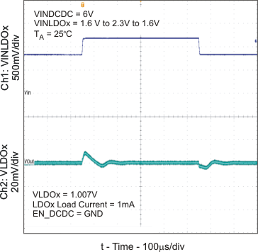 Figure 9. Line Transient Response (LDOx)
 Figure 11. Load Transient Response (DC-DC PWM Mode)
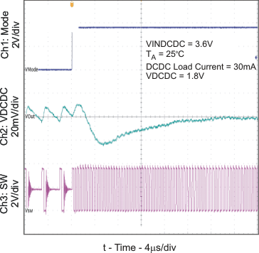 Figure 13. PFM to PWM Transition (DC-DC)
 Figure 15. Power-Supply Rejection Ratio (LDOx) vs Frequency
 Figure 2. Efficiency (DC-DC 600-mA PWM Mode)
vs Output Current
 Figure 4. Output Voltage Ripple (DC-DC PWM Mode)
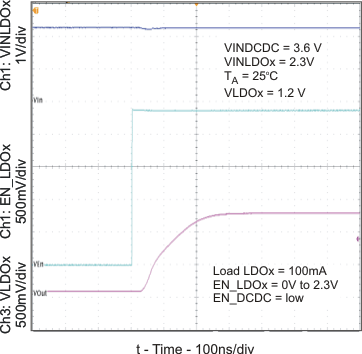 Figure 6. Start-Up Timing (LDOx)
 Figure 8. Line Transient Response (DC-DC PWM Mode)
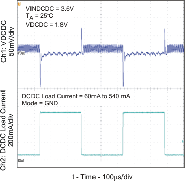 Figure 10. Load Transient Response (DC-DC PFM Mode)
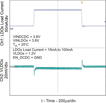 Figure 12. Load Transient Response (LDOx)
 Figure 14. PWM to PFM Transition (DC-DC)