SLVS810C June 2009 – September 2015 TPS65000 , TPS650001 , TPS650003 , TPS650006 , TPS65001 , TPS650061
PRODUCTION DATA.
- 1 Features
- 2 Applications
- 3 Description
- 4 Revision History
- 5 Description (continued)
- 6 Device Options
- 7 Pin Configuration and Functions
- 8 Specifications
- 9 Detailed Description
- 10Application and Implementation
- 11Power Supply Recommendations
- 12Layout
- 13Device and Documentation Support
- 14Mechanical, Packaging, and Orderable Information
Package Options
Mechanical Data (Package|Pins)
- RTE|16
Thermal pad, mechanical data (Package|Pins)
- RTE|16
Orderable Information
9 Detailed Description
9.1 Overview
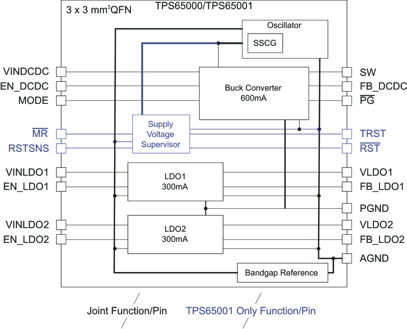
The TPS6500x provides one step-down converter, two low dropout regulators, spread spectrum clock generation, and a supply voltage supervisor for the TPS65001 only. The device has an input voltage range of
2.3 V to 6 V and is characterized across a –40°C to 85°C range. This device is intended, but not limited, to powering smart phones, embedded processors, and point-of-load devices.
The output voltage of the step-down converter can be selected through resistor networks on the output. To maximize efficiency, there are two modes of operation based on load conditions: PWM or PFM. By pulling the MODE pin high, forced PWM can be achieved. Pulling this pin low results in an automatic adjustment between PFM and PWM modes.
The two general purpose low drop-out regulators each have their own separate enables and voltage inputs. The inputs can be tied to the output of the step-down converter or to a separate voltage source. Resistor networks are required on the output of the regulator to set the output voltage. Their wide voltage range lets them handle direct connections to a battery.
The switching frequency of the step-down converter is handled by the oscillator, with a typical frequency of
2.25 MHz. The spread spectrum clock (SSC) modulates this frequency when the device is in PWM mode. This additional circuit in the oscillator block reduces power that may cause EMI.
The TPS6500x devices also provide a power good signal to monitor the condition of the DC-DC and both LDOs. The DC-DC and LDOs are only monitored if their enable signal is high. If all enabled resources are in regulation, the pin is pulled low. If one or more of the enabled resources are out of regulation, the pin is pulled in Hi-Z.
The supply voltage supervisor is only available for the TPS65001 and TPS650061 devices. This circuit monitors the supply voltage to the device that the TPS65001 and TPS650061 is powering for under voltage conditions. The circuit can connect to a button for manual resets. Reset-recovery time can also be set. Four different scenarios can trigger the circuit to cause a rest.
9.2 Functional Block Diagram
9.3 Feature Description
9.3.1 Step-Down Converter
TI intends the step-down converter to maximize the flexibility in the equipment. The output voltage is selectable with a resistor network on the output. Figure 15 shows the required connections.
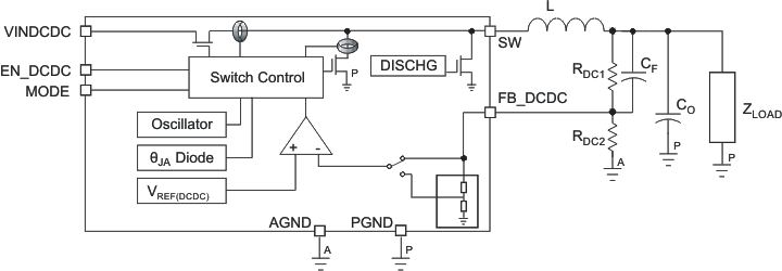 Figure 15. DCDC Block Diagram and Output Voltage Setting
The output voltage of the DC-DC converter is set by Equation 1:
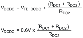
The combined resistance of RDC1 and RDC2 should be less than 1 MΩ.
Fixed output voltages and additional current limit options are also possible. Contact TI for further information.
The step-down converter has two modes of operation to maximize efficiency at different load conditions. At moderate to heavy load currents, the device operates in a fixed-frequency pulse width modulation (PWM) mode that results in small output ripple and high efficiency. Pulling the MODE pin to a DC-high level results in PWM mode over the load range.
At light-load currents, the device operates in a pulsed-frequency modulation (PFM) mode to improve efficiency. The transition to this mode occurs when the inductor current through the low-side FET becomes zero, indicating discontinuous conduction. PFM mode also results in the output voltage increasing by 1% from its nominally set value. TI intends this voltage positioning to minimize the voltage undershoot of a load step from light to heavy loads, as when a processor moves from sleep to active modes, and the voltage overshoot at load throw-off. Figure 16 shows the voltage positioning behavior for a light to heavy load step.
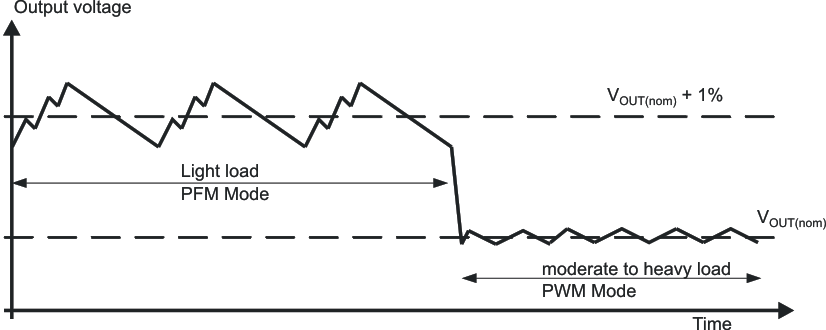 Figure 16. PFM Voltage Positioning
Pulling the MODE pin to DC ground results in an automatic transition between PFM and PWM modes to maximize efficiency.
The DC-DC converter output automatically discharges to ground through an internal 450-Ω load when EN_DCDC goes low or when the UVLO condition is met.
9.3.2 Soft Start
The step-down converter has an internal soft start circuit that limits the inrush current during start-up. During a soft start, the output voltage ramp up is controlled as Figure 17 shows.
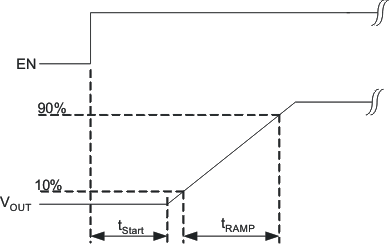 Figure 17. Soft Start
9.3.3 Linear Regulators
TI designed the two linear drop-out regulators (LDOs) in the TPS65000 and TPS65001 to provide flexibility in system design. Each LDO has a separate voltage input and enable signal. The input can be tied to the output of the step-down converter or the output of another voltage source. Each LDO output discharge to ground automatically when EN_LDOx goes low.
A resistor network is required to set the output voltage of the LDOs. Fixed-voltage output versions are also available. Contact TI sales representative for more information.
The LDOs are general-purpose devices that can handle inputs from 6 V to 1.6 V, making them suitable for directly connecting to the battery. Figure 18 illustrates the connections for LDO1. The same architecture applies to LDO2.
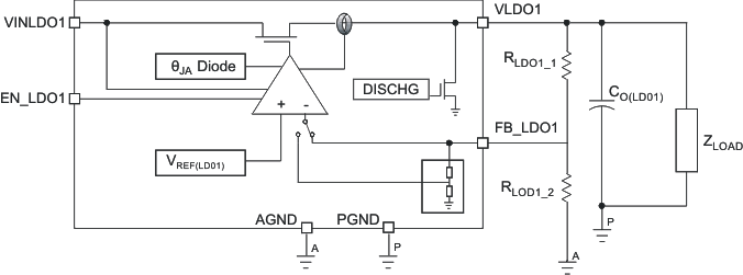 Figure 18. LDO Block Diagram and Output Voltage Setting
The output voltages of the LDOs are set by Equation 2:
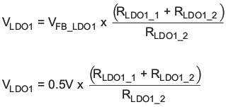
The combined resistance of RLDO1_1 and RLDO1_2 should be less than 1 MΩ.
9.3.4 Oscillator and Spread Spectrum Clock Generation
The TPS6500x contains an internal oscillator running at a typical frequency of 2.25 MHz. This frequency is the fundamental switching frequency of the step-down converter when running in PWM mode. An additional circuit in the oscillator block implements spread spectrum clocking, which modulates the main-switching frequency when the device is in PWM mode. This spread spectrum oscillation reduces the power that may cause EMI. When viewed in the frequency domain, the SSC spreads out the frequency that may introduce interference while simultaneously reducing the power. Because the frequency is continually shifting, the amount of time the switcher spends at any single frequency is reduced. This reduction in time indicates that the receiver that may sense the interference has less time to integrate the interference.
Different spin versions of SSC settings are also feasible. Contact a TI sales representative for more information.
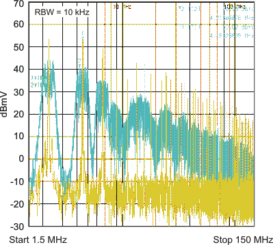 Figure 19. SSC On/Off Comparison from 1.5 MHz to 150 MHz
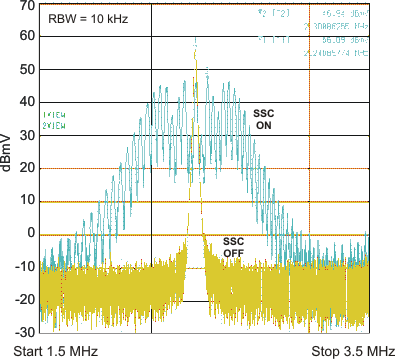 Figure 20. Zoom In of SSC On/Off Comparison from 1.5 MHz to 3.5 MHz
Figure 19 to Figure 20 shows the advantage of SSC with the frequency spectrum centering on the nominal frequency 2.25 MHz. The blue spectrum is the result of the spread change. The figures show the harmonic spectrum is attenuated 10 dB comparing to the same device without SSC.
9.3.5 Power Good
The open drain PG output indicates the condition of the step-down converter and each LDO. This output is combined, with the outputs being compared when the appropriate enable signal is high. The pin is pulled low when all enabled outputs are greater than 90% of the target voltage and Hi-Z when an enabled output is less than 90% of its intended value or when all the enable signals are pulled low.
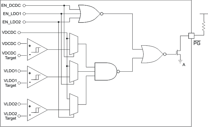 Figure 21. Power Good Functionality
9.3.6 Supply Voltage Supervisor (SVS) [TPS65001 and TPS650061 Only]
The SVS has fourinputs and one output. The RST pin is an active-low high-impedance output. The MR pin is an active-low input that suitable for connecting to a push-button circuit for manual reset generation. The RSTSNS pin is an analog-input pin for voltage comparison. The TRST pin is connected to an external capacitor, allowing the reset timing to be set in the application. The VINDCDC pin is the main-supply input for the control circuits and the switch-mode converter.
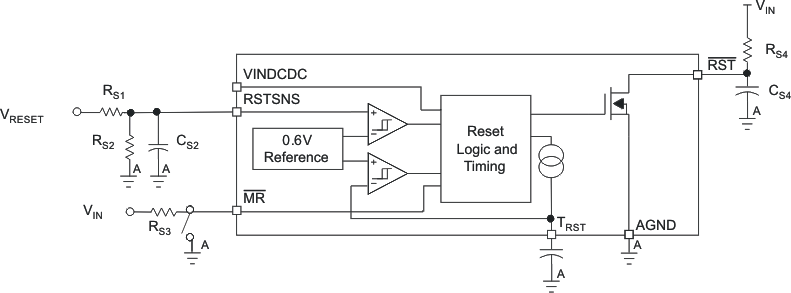 Figure 22. SVS Block Diagram
Each input can individually trigger RST to go active. Table 1 outlines the paths to activate the reset.
Table 1. RST Generation Table
| INPUTS | OUTPUTS | ||
|---|---|---|---|
| VINDCDC | MR | VRSTSNS | RST |
| 0.4 < V < UVLO | X | X | Low |
| > UVLO | ≥ VIH(MR) | ≤ 0.6 V | Low |
| > UVLO | ≥ VIH(MR) | > 0.6 V | High-Z |
| > UVLO | < VIL(MR) | X | Low |
The RSTSNS pin must be tied to VINDCDC if the reset functionality is not required from this pin. This action causes the reset to activate only when VINDCDC is rising from 0 V or when VINDCDC drops below UVLO. The RSTSNS pin must connect to an external RC network to set the deglitch timing for triggering a reset when VINDCDC is below the UVLO threshold. The reset threshold voltage is given by Equation 3:

The RST recovery timing is set by the capacitor on the TRST pin. A 2-μA current is enabled when the reset condition is met, charging the capacitor. The TRST voltage is monitored internally and the reset ends when the voltage reaches 0.6 V. The capacitor value to reset time can be computed with Equation 4:

The value tRST is the time from the end of condition that activated RST until RST returns to its Hi-Z state. The TRST pin would be internally discharged to ground when the reset condition is true or after tRST.
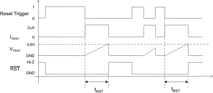 Figure 23. RST Recovery Timing
9.4 Device Functional Modes
The step-down converter has two modes of operation to maximize efficiency:
PFM
- For light loads
- For automatic transition to between this mode and PWM mode automatically when MODE pin is pulled low over all load ranges
- To increase in output voltage setting by 1%
- For better accuracy
PWM
- For moderate to heavy loads
- For a small output ripple
- For pulling MODE pin high to result in PWM mode over all load range