SLVSAE3A August 2010 – January 2016 TPS650231
PRODUCTION DATA.
- 1 Features
- 2 Applications
- 3 Description
- 4 Revision History
- 5 Description (continued)
- 6 Pin Configuration and Functions
-
7 Specifications
- 7.1 Absolute Maximum Ratings
- 7.2 ESD Ratings
- 7.3 Recommended Operating Conditions
- 7.4 Thermal Information
- 7.5 Electrical Characteristics
- 7.6 Electrical Characteristics: Control Signals
- 7.7 Electrical Characteristics: Supply Pins VCC, VINDCDC1, VINDCDC2, VINDCDC3, VINDCDC13
- 7.8 Electrical Characteristics: Supply Pins VBACKUP, VSYSIN, VRTC, VINLDO
- 7.9 Electrical Characteristics: VDCDC1 Step-Down Converter
- 7.10 Electrical Characteristics: VDCDC2 Step-Down Converter
- 7.11 Electrical Characteristics: VDCDC3 Step-Down Converter
- 7.12 Timing Requirements
- 7.13 Typical Characteristics
-
8 Detailed Description
- 8.1 Overview
- 8.2 Functional Block Diagrams
- 8.3
Feature Description
- 8.3.1 VRTC Output and Operation With or Without Backup Battery
- 8.3.2 Step-Down Converters, VDCDC1, VDCDC2, and VDCDC3
- 8.3.3 Power Save Mode Operation
- 8.3.4 Low-Ripple Mode
- 8.3.5 Soft-Start
- 8.3.6 100% Duty Cycle Low-Dropout Operation
- 8.3.7 Active Discharge When Disabled
- 8.3.8 Power-Good Monitoring
- 8.3.9 Low-Dropout Voltage Regulators
- 8.3.10 Undervoltage Lockout
- 8.3.11 Power-Up Sequencing
- 8.3.12 System Reset + Control Signals
- 8.4 Device Functional Modes
- 8.5 Programming
- 8.6
Register Maps
- 8.6.1 VERSION Register Address: 00h (Read Only)
- 8.6.2 PGOODZ Register Address: 01h (Read Only)
- 8.6.3 MASK Register Address: 02h (Read or Write), Default Value: C0h
- 8.6.4 REG_CTRL Register Address: 03h (Read or Write), Default Value: FFh
- 8.6.5 CON_CTRL Register Address: 04h (Read or Write), Default Value: B1h
- 8.6.6 CON_CTRL2 Register Address: 05h (Read or Write), Default Value: 40h
- 8.6.7 DEFCORE Register Address: 06h (Read or Write), Default Value: 14h/1Eh
- 8.6.8 DEFSLEW Register Address: 07h (Read or Write), Default Value: 06h
- 8.6.9 LDO_CTRL Register Address: 08h (Read or Write), Default Value: Set with DEFLDO1 and DEFLDO2
- 9 Application and Implementation
- 10Power Supply Recommendations
- 11Layout
- 12Device and Documentation Support
- 13Mechanical, Packaging, and Orderable Information
Package Options
Mechanical Data (Package|Pins)
Thermal pad, mechanical data (Package|Pins)
- RSB|40
Orderable Information
9 Application and Implementation
NOTE
Information in the following applications sections is not part of the TI component specification, and TI does not warrant its accuracy or completeness. TI’s customers are responsible for determining suitability of components for their purposes. Customers should validate and test their design implementation to confirm system functionality.
9.1 Application Information
9.1.1 Input Voltage Connection
The low power section of the control circuit for the step-down converters DCDC1, DCDC2, and DCDC3 is supplied by the VCC pin while the circuitry with high power such as the power stage is powered from the VINDCDC1, VINDCDC2, and VINDCDC3 pins. For proper operation of the step-down converters, VINDCDC1, VINDCDC2, VNDCDC3, and VCC need to be tied to the same voltage rail. Step-down converters that are planned to be not used, still need to be powered from their input pin on the same rails than the other step-down converters and VCC.
LDO1 and LDO2 share a supply voltage pin which can be powered from the VCC rails or from a voltage lower than VCC, for example, the output of one of the step-down converters as long as it is operated within the input voltage range of the LDOs. If both LDOs are not used, the VINLDO pin can be tied to GND.
9.1.2 Unused Regulators
In case a step-down converter is not used, its input supply voltage pin VINDCDCx still must be connected to the VCC rail along with supply input of the other step-down converters. TI recommends closing the control loop such that an inductor and output capacitor is added in the same way as it would be when operated normally. If one of the LDOs is not used, its output capacitor must be added as well. If both LDOs are not used, the input supply pin as well as the output pins of the LDOs (VINLDO, VLDO1, VLDO2) must be tied to GND.
9.1.3 Reset Condition of DCDC1
If DEFDCDC1 is connected to ground and DCDC1_EN is pulled high after VINDCDC1 is applied, the output voltage of DCDC1 defaults to 1.225 V instead of 1.2 V (high by 2%). Figure 38 illustrates the problem.
 Figure 38. Default DCDC1
One workaround is to tie DCDC1_EN to VINDCDC1 (Figure 39).
 Figure 39. Workaround 1
Another workaround is to write the correct voltage to the DEF_CORE register through I2C. This can be done before or after the converter is enabled. If written before the enable, the only bit changed is DEF_CORE[0]. The voltage is 1.2 V, however, when the enable is pulled high (Figure 40).
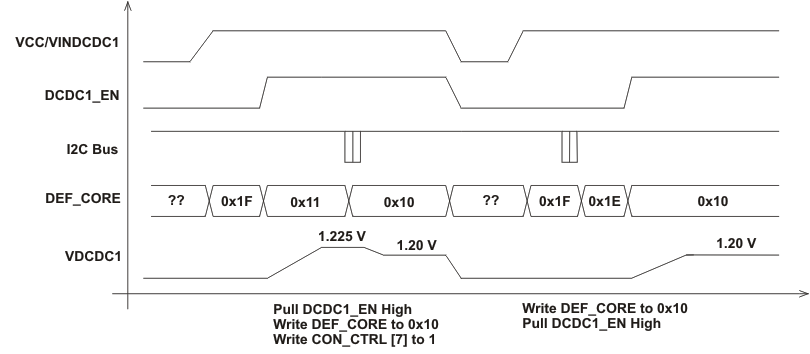 Figure 40. Workaround 2
A third workaround is to generate a HOT_RESET after enabling DCDC1 (Figure 41).
 Figure 41. Workaround 3
Table 17. Differences of TPS650231 vs TPS65023 and TPS65023B
| ITEM | DESCRIPTION | TPS65023 | TPS65023B | TPS650231 |
|---|---|---|---|---|
| VIH | High level input voltage for the SDAT pin | Minimum 1.3 V | Minimum 1.65 V; Vcc = 2.5 V to 5.25 V |
Minimum 1.65 V; Vcc = 2.5 V to 5.25 V |
| VIH | High level input voltage for the SCLK pin | Minimum 1.3 V | Minimum 1.4 V, Vcc = 2.5 V to 5.25 V |
Minimum 1.4 V, Vcc = 2.5 V to 5.25 V |
| VIL | Low level input voltage for SCLK and SDAT pin | Maximum 0.4 V | Maximum 0.35 V | Maximum 0.35 V |
| th(DATA) | Data input hold time | Minimum 300 ns | Minimum 100 ns | Minimum 100 ns |
| tsu(DATA) | Data input setup time | Minimum 300 ns | Minimum 100 ns | Minimum 100 ns |
| LDO1 voltage for setting LDO1_[2..0] = 011 | 1.8 V | 1.8 V | 2.1 V | |
| DEFDCDC2 pin functionality | 1) DEFDCDC2 = LOW: Vo = 1.8 V 2) DEFDCDC2 = HIGH: Vo = 3.3 V 3) 0.6 V feedback input |
1) DEFDCDC2 = LOW: Vo = 1.8 V 2) DEFDCDC2 = HIGH: Vo = 3.3 V 3) 0.6 V feedback input |
0.6 V feedback input only (allows voltage scaling with external resistor divider without restrictions) |
9.2 Typical Application
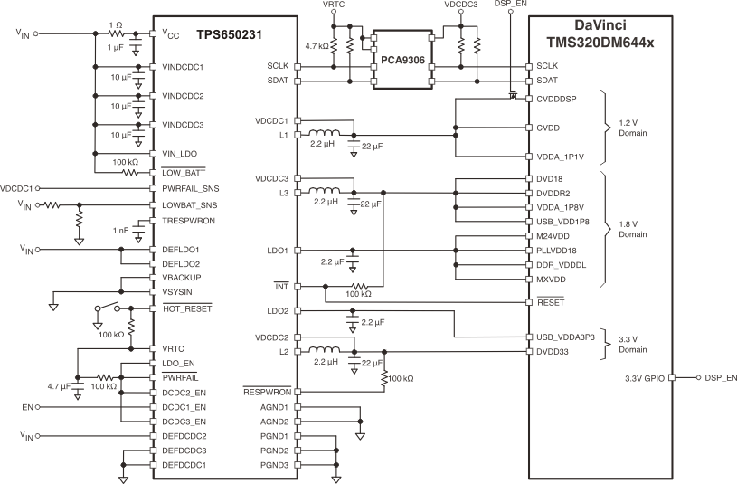 Figure 42. Typical Configuration for the Texas Instruments TMS320DM644x DaVinci Processors
9.2.1 Design Requirements
The TPS650231 device has only a few design requirements. Use the following parameters for the design examples:
- 1-μF bypass capacitor on VCC, located as close as possible to the VCC pin to ground
- VCC and VINDCDCx must be connected to the same voltage supply with minimal voltage difference
- Input capacitors must be present on the VINDCDCx and VIN_LDO supplies if used
- Output inductor and capacitors must be used on the outputs of the DCDC converters if used
- Output capacitors must be used on the outputs of the LDOs if used
9.2.2 Detailed Design Procedure
9.2.2.1 Inductor Selection for the DC-DC Converters
Each of the converters in the TPS650231 typically use a 2.2-μH output inductor. Larger or smaller inductor values are used to optimize the performance of the device for specific operation conditions. The selected inductor has to be rated for its DC resistance and saturation current. The DC resistance of the inductance influences directly the efficiency of the converter. Therefore, an inductor with lowest DC resistance must be selected for highest efficiency.
For a fast transient response, a 2.2-μH inductor in combination with a 22-μF output capacitor is recommended.
Equation 8 calculates the maximum inductor current under static load conditions. The saturation current of the inductor must be rated higher than the maximum inductor current as calculated with Equation 8. This is needed because during heavy-load transient the inductor current rises above the value calculated under Equation 8.


where
- f = Switching frequency (2.25 MHz typical)
- L = Inductor value
- ΔIL = Peak-to-peak inductor ripple current
- ILMAX = Maximum inductor current
The highest inductor current occurs at maximum Vin.
Open-core inductors have a soft saturation characteristic, and they can usually handle higher inductor currents versus a comparable shielded inductor.
A more conservative approach is to select the inductor current rating just for the maximum switch current of the TPS650231 (2 A for the VDCDC1 and VDCDC2 converters, and 1.5 A for the VDCDC3 converter). The core material from inductor to inductor differs and has an impact on the efficiency especially at high switching frequencies.
See Table 18 and the typical applications for possible inductors.
Table 18. Tested Inductors
| DEVICE | INDUCTOR VALUE | TYPE | COMPONENT SUPPLIER |
|---|---|---|---|
| All Converters | 2.2 μH | LPS4012-222LMB | Coilcraft |
| 2.2 μH | VLCF4020T-2R2N1R7 | TDK | |
| For DCDC2 or DCDC3 | 2.2 μH | LQH32PN2R2NN0 | Murata |
| 2.2 μH | PSI25201T-2R2 | Cyntec | |
| For DCDC1 | 1.5 μH | LQH32PN1R5NN0 | Murata |
9.2.2.2 Output Capacitor Selection
The advanced fast response voltage mode control scheme of the inductive converters implemented in the TPS650231 allow the use of small ceramic capacitors with a typical value of 10 μF for each converter without having large output voltage under and overshoots during heavy load transients. Ceramic capacitors with low ESR values have the lowest output voltage ripple and are recommended. See Table 19 for recommended components.
If ceramic output capacitors are used, the capacitor RMS ripple current rating always meets the application requirements. Just for completeness, the RMS ripple current is calculated with Equation 10.

At nominal load current, the inductive converters operate in PWM mode. The overall output voltage ripple is the sum of the voltage spike caused by the output capacitor ESR plus the voltage ripple caused by charging and discharging the output capacitor in Equation 11.

where
- the highest output voltage ripple occurs at the highest input voltage Vin
At light-load currents, the converters operate in PSM and the output voltage ripple is dependent on the output capacitor value. The output voltage ripple is set by the internal comparator delay and the external capacitor. The typical output voltage ripple is less than 1% of the nominal output voltage.
9.2.2.3 Input Capacitor Selection
Because of the nature of the buck converter having a pulsating input current, a low-ESR input capacitor is required for best input voltage filtering and minimizing the interference with other circuits caused by high input voltage spikes. Each DC-DC converter requires a 10-μF ceramic input capacitor on its input pin VINDCDCx. The input capacitor is increased without any limit for better input voltage filtering. The VCC pin is separated from the input for the DC-DC converters. A filter resistor of up to 10R and a 1-μF capacitor is used for decoupling the VCC pin from switching noise.
NOTE
The filter resistor may affect the UVLO threshold because up to 3 mA can flow through this resistor into the VCC pin when all converters are running in PWM mode.
Table 19. Possible Capacitors
| CAPACITOR VALUE | CASE SIZE | COMPONENT SUPPLIER | COMMENTS |
|---|---|---|---|
| 22 μF | 0805 | TDK C2012X5R0J226MT | Ceramic |
| 22 μF | 0805 | Taiyo Yuden JMK212BJ226MG | Ceramic |
| 10 μF | 0805 | Taiyo Yuden JMK212BJ106M | Ceramic |
| 10 μF | 0805 | TDK C2012X5R0J106M | Ceramic |
| 10 μF | 0603 | Taiyo Yuden JMK107BJ106 | Ceramic |
9.2.2.4 Output Voltage Selection
The DEFDCDC1, DEFDCDC2, and DEFDCDC3 pins are used to set the output voltage for each step-down converter. For DEFDCDC1 and DEFDCDC3 there are default voltages defined when the pin is tied to a logic low or logic high signal. See Table 20 for the default voltages if the pins are pulled to GND or to Vcc. If a different voltage is needed, an external resistor divider can be added to the DEFDCDCx pin as shown in Figure 43.
The output voltage of VDCDC1 is set with the I2C interface. If the voltage is changed from the default, using the DEFCORE register, the output voltage only depends on the register value. Any resistor divider at DEFDCDC1 can not change the voltage set with the register. TI does not recommend changing the divider ratio of a resistor divider connected at DEFDCDC1 or DEFDCDC3 during operation as the internal logic may detect a logic high signal in error during the change from a high voltage to a lower voltage and scales the output to the voltage defined by DEFDCDCx = HIGH. As DEFDCDC2 does not have these default fixed voltages, the resistor divider can be changed during operation.
Table 20. DCDC1 and DCDC3 Default Voltage Levels
| PIN | LEVEL | DEFAULT OUTPUT VOLTAGE |
|---|---|---|
| DEFDCDC1 | VCC | 1.6 V |
| GND | 1.2 V | |
| DEFDCDC3 | VCC | 3.3 V |
| GND | 1.8 V |
This function is not available on the DCDC2 converter. DEFDCDC2 always needs to be connected to a resistive divider.
Using an external resistor divider for the DEFDCDCx is shown in Figure 43.
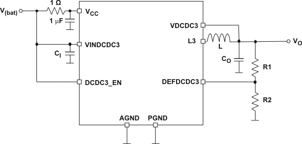 Figure 43. External Resistor Divider
When a resistor divider is connected to DEFDCDCx, the output voltage can be set from 0.6 V up to the input voltage V(bat). The total resistance (R1+R2) of the voltage divider must be kept in the 1-MΩ range to maintain a high efficiency at light load.
V(DEFDCDCx) = 0.6 V

9.2.2.5 VRTC Output
It is required to add a capacitor of 4.7-μF minimum to the VRTC pin, even the output may be unused.
9.2.2.6 LDO1 and LDO2
The LDOs in the TPS650231 are general-purpose LDOs which are stable using ceramics capacitors. The minimum output capacitor required is 2.2 μF. The LDOs output voltage can be changed to different voltages between 1 V and 3.3 V using the I2C interface. The supply voltage for the LDOs needs to be connected to the VINLDO pin, giving the flexibility to connect the lowest voltage available in the system and provides the highest efficiency.
9.2.2.7 TRESPWRON
This is the input to a capacitor that defines the reset delay time after the voltage at VRTC rises above 2.52 V. The timing is generated by charging and discharging the capacitor with a current of 2 μA between a threshold of 0.25 V and 1 V for 128 cycles. A 1-nF capacitor gives a delay time of 100 ms.
While there is no real upper and lower limit for the capacitor connected to TRESPWRON, TI recommends to not leave signal pins open.

where
- t(reset) is the reset delay time
- C(reset) is the capacitor connected to the TRESPWRON pin
The minimum and maximum values for the timing parameters called ICONST (2 μA), TRESPWRON_UPTH (1 V) and TRESPWRON_LOWTH (0.25 V) can be found in Specifications.
9.2.2.8 VCC Filter
An RC filter connected at the VCC input is used to keep noise from the internal supply for the bandgap and other analog circuitry. A typical value of 1 Ω and 1 μF is used to filter the switching spikes, generated by the DC-DC converters. A larger resistor than 10 Ω must not be used because the current into VCC of up to 3 mA causes a voltage drop at the resistor causing the undervoltage lockout circuitry connected at VCC internally to switch off too early.
9.2.3 Application Curves
Graphs were taken using the EVM with the following inductor and output capacitor combinations:
| CONVERTER | INDUCTOR | OUTPUT CAPACITOR | OUTPUT CAPACITOR VALUE |
|---|---|---|---|
| VDCDC1 | LQH32PN1R5 | JMK107BJ106 | 2 × 10 μF |
| VDCDC2 | LQH32PN2R2 | JMK107BJ106 | 2 × 10 μF |
| VDCDC3 | LQH32PN2R2 | JMK107BJ106 | 2 × 10 μF |
space
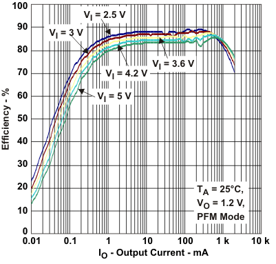 Figure 44. DCDC1: Efficiency vs Output Current
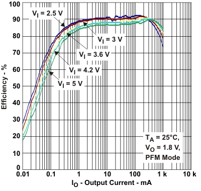 Figure 46. DCDC3: Efficiency vs Output Current
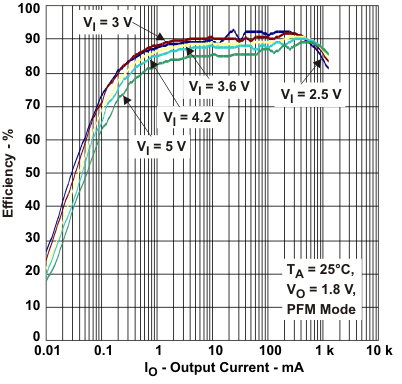 Figure 45. DCDC2: Efficiency vs Output Current