SLVS774C June 2007 – January 2016 TPS650240 , TPS650241 , TPS650242 , TPS650243 , TPS650244 , TPS650245
PRODUCTION DATA.
- 1 Features
- 2 Applications
- 3 Description
- 4 Revision History
- 5 Description (continued)
- 6 Pin Configuration and Functions
-
7 Specifications
- 7.1 Absolute Maximum Ratings
- 7.2 ESD Ratings
- 7.3 Recommended Operating Conditions
- 7.4 Thermal Information
- 7.5 Electrical Characteristics: Control Signals and Supply Pins
- 7.6 Electrical Characteristics: VDCDC1 Step-Down Converter
- 7.7 Electrical Characteristics: VDCDC2 Step-Down Converter
- 7.8 Electrical Characteristics: VDCDC3 Step-Down Converter
- 7.9 Electrical Characteristics: General
- 7.10 Typical Characteristics
- 8 Detailed Description
- 9 Application and Implementation
- 10Power Supply Recommendations
- 11Layout
- 12Device and Documentation Support
- 13Mechanical, Packaging, and Orderable Information
Package Options
Mechanical Data (Package|Pins)
- RHB|32
Thermal pad, mechanical data (Package|Pins)
- RHB|32
Orderable Information
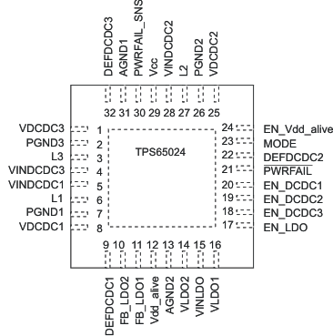
6 Pin Configuration and Functions
RHB Package
32-Pin VQFN
Top View

Pin Functions
| PIN | I/O | DESCRIPTION | |
|---|---|---|---|
| NAME | NO. | ||
| SWITCHING REGULATOR SECTION | |||
| AGND1 | 31 | – | Analog ground connection. All analog ground pins are connected internally on the chip. |
| AGND2 | 13 | – | Analog ground connection. All analog ground pins are connected internally on the chip. |
| 9 | I | Input signal indicating default VDCDC1 voltage, 0 = 2.80 V, 1 = 3.3 V | |
| DEFDCDC1 | This pin can also be connected to a resistor divider between VDCDC1 and GND. In this case the output voltage of the DCDC1 converter can be set in a range from 0.6V to VINDCDC1 | ||
| 22 | I | Input signal indicating default VDCDC2 voltage, 0 = 1.8 V, 1 = 2.5 V | |
| DEFDCDC2 | This pin can also be connected to a resistor divider between VDCDC2 and GND. In this case the output voltage of the DCDC2 converter can be set in a range from 0.6V to VINDCDC2. | ||
| DEFDCDC3 | 32 | I | Input signal indicating VDCDC3 voltage. TPS650240: 0 = 1.0 V, 1 = 1.3 V TPS650241: 0 = 0.9 V, 1 = 1.375 V TPS650242: 0 = 1.0 V, 1 = 1.5 V TPS650243: 0 = 1.0 V, 1 = 1.2 V TPS650244: 0 = 1.55 V, 1 = 1.6 V TPS650245: 0 = 0.9 V, 1 = 1.1 V |
| EN_DCDC1 | 20 | I | VDCDC1 enable pin. A logic high enables the regulator, a logic low disables the regulator. |
| EN_DCDC2 | 19 | I | VDCDC2 enable pin. A logic high enables the regulator, a logic low disables the regulator. |
| EN_DCDC3 | 18 | I | VDCDC3 enable pin. A logic high enables the regulator, a logic low disables the regulator. |
| L1 | 6 | – | Switch pin of VDCDC1 converter. The VDCDC1 inductor is connected here. |
| L2 | 27 | – | Switch pin of VDCDC2 converter. The VDCDC2 inductor is connected here. |
| L3 | 3 | – | Switch pin of VDCDC3 converter. The VDCDC3 inductor is connected here. |
| PGND1 | 7 | – | Power ground for VDCDC1 converter |
| PGND2 | 26 | – | Power ground for VDCDC2 converter |
| PGND3 | 2 | – | Power ground for VDCDC3 converter |
| PowerPad | – | – | Connect the power pad to analog ground |
| VCC | 29 | I | Power supply for digital and analog circuitry of DCDC1, DCDC2, and DCDC3 DC-DC converters. This must be connected to the same voltage supply as VINDCDC3, VINDCDC1, and VINDCDC2. |
| VDCDC1 | 8 | I | VDCDC1 feedback voltage sense input, connect directly to VDCDC1 |
| VDCDC2 | 25 | I | VDCDC2 feedback voltage sense input, connect directly to VDCDC2 |
| VDCDC3 | 1 | I | VDCDC3 feedback voltage sense input, connect directly to VDCDC3 |
| VINDCDC1 | 5 | I | Input voltage for VDCDC1 step-down converter. This must be connected to the same voltage supply as VINDCDC2, VINDCDC3, and VCC. |
| VINDCDC2 | 28 | I | Input voltage for VDCDC2 step-down converter. This must be connected to the same voltage supply as VINDCDC1, VINDCDC3, and VCC. |
| VINDCDC3 | 4 | I | Input voltage for VDCDC3 step-down converter. This must be connected to the same voltage supply as VINDCDC1, VINDCDC2, and VCC. |
| LDO REGULATOR SECTION | |||
| EN_LDO | 17 | I | Enable input for LDO1 and LDO2. Logic high enables the LDOs, logic low disables the LDOs. |
| EN_Vdd_alive | 24 | I | Enable input for Vdd_alive LDO. Logic high enables the LDO, logic low disables the LDO. |
| FB_LDO1 | 11 | I | Feedback pin for LDO1 |
| FB_LDO2 | 10 | I | Feedback pin for LDO2 |
| Vdd_alive | 12 | O | Output voltage for Vdd_alive |
| VINLDO | 15 | I | Input voltage for LDO1 and LDO2 |
| VLDO1 | 16 | O | Output voltage of LDO1 |
| VLDO2 | 14 | O | Output voltage of LDO2 |
| CONTROL AND I2C SECTION | |||
| MODE | 23 | I | Select between power safe mode and forced PWM mode for DCDC1, DCDC2, and DCDC3. In power safe mode PFM is used at light loads, PWM for higher loads. If PIN is set to high level, forced PWM mode is selected. If the pin has low level, then the device operates in power safe mode. |
| PWRFAIL | 21 | O | Open-drain output. Active low when PWRFAIL comparator indicates low VBAT condition. |
| PWRFAIL_SNS | 30 | I | Input for the comparator driving the PWRFAIL output |