SLVS843B December 2008 – May 2018 TPS650250
PRODUCTION DATA.
- 1 Features
- 2 Applications
- 3 Description
- 4 Revision History
- 5 Pin Configuration and Functions
-
6 Specifications
- 6.1 Absolute Maximum Ratings
- 6.2 ESD Ratings
- 6.3 Recommended Operating Conditions
- 6.4 Thermal Information
- 6.5 Dissipation Ratings
- 6.6 Electrical Characteristics
- 6.7 Electrical Characteristics VDCDC1
- 6.8 Electrical Characteristics VDCDC2
- 6.9 Electrical Characteristics VDCDC3
- 6.10 Typical Characteristics
- 7 Detailed Description
- 8 Application and Implementation
- 9 Power Supply Recommendations
- 10Layout
- 11Device and Documentation Support
- 12Mechanical, Packaging, and Orderable Information
Package Options
Mechanical Data (Package|Pins)
- RHB|32
Thermal pad, mechanical data (Package|Pins)
- RHB|32
Orderable Information
7.3.2 Power Save Mode Operation
As the load current decreases, the converters enter Power Save Mode operation. During Power Save Mode the converters operate in a burst mode (PFM mode) with a frequency between 1.125 MHz and 2.25 MHz for one burst cycle. However, the frequency between different burst cycles depends on the actual load current and is typically far less than the switching frequency, with a minimum quiescent current to maintain high efficiency.
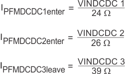
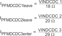
In order to optimize the converter efficiency at light load the average current is monitored and if in PWM mode the inductor current remains below a certain threshold, then Power Save Mode is entered. The typical threshold to enter Power Save Mode can be calculated as follows:

During Power Save Mode the output voltage is monitored with a comparator and by maximum skip burst width. As the output voltage falls below the threshold, set to the nominal VO, the P-channel switch turns on and the converter effectively delivers a constant current as defined below.

If the load is below the delivered current then the output voltage rises until the same threshold is crossed in the other direction. All switching activity ceases, reducing the quiescent current to a minimum until the output voltage has again dropped below the threshold. The power save mode is exited, and the converter returns to PWM mode if either of the following conditions are met:
- The output voltage drops 2% below the nominal VO due to increased load current
- The PFM burst time exceeds 16 × 1/fs (7.1μs typical)
These control methods reduce the quiescent current to typically 14μA per converter and the switching activity to a minimum thus achieving the highest converter efficiency. Setting the comparator thresholds at the nominal output voltage at light load current results in a very low output voltage ripple. The ripple depends on the comparator delay and the size of the output capacitor; increasing capacitor values makes the output ripple tend to zero. Power Save Mode can be disabled by pulling the MODE pin high. This forces all DC-DC converters into fixed frequency PWM mode.