SLVSCF4A December 2014 – July 2016 TPS650830
PRODUCTION DATA.
- 1 Device Overview
- 2 Revision History
- 3 Device Options
- 4 Pin Configuration and Functions
- 5 Specifications
-
6 Detailed Description
- 6.1 Overview
- 6.2 Functional Block Diagram
- 6.3
Feature Description
- 6.3.1 Voltage Regulator Assignment and Powergood Comparator Logic Assignment (External Voltage Regulator or Load Switch) for Skylake and Kabylake Platform
- 6.3.2 Generic Powergood Window Comparator with Open-Drain Output
- 6.3.3 Powergood Window Comparator
- 6.3.4 3.3-V LDO and 3V3SW Load Switch
- 6.3.5 5-V LDO and 5VSW Load Switch
- 6.3.6 RTC Selector and 3.1-V LDO
- 6.3.7 Power Path Comparators
- 6.3.8 UVLO Comparators
- 6.3.9 Temperature Comparator
- 6.3.10 Low Power Mode (LPM) / Connected Standby / Instant Go of VRs
- 6.3.11 Enable and Powergood of VRs
- 6.3.12 VR4 VDDQ and LDO1 VTT Enabling
- 6.3.13
Converters
- 6.3.13.1 Power Save Mode
- 6.3.13.2 Voltage Regulator Startup
- 6.3.13.3 Powergood, Power Fault, and Emergency Power Shutdown
- 6.3.13.4 Current Limit
- 6.3.13.5 Output Discharge Feature
- 6.3.13.6 Output Voltage Control
- 6.3.13.7 Converter Low Power Mode Operation
- 6.3.13.8 Controller Low Power Mode Operation
- 6.3.13.9 Controller Internal Ramp Comparator
- 6.3.13.10 Undervoltage Lockout
- 6.3.14 Coincell Selector
- 6.4 Device Functional Modes
- 6.5 Programming
- 6.6
Register Map
- 6.6.1
Registers
- 6.6.1.1 VENDORID Register (address = 0x00) [reset = 00100010]
- 6.6.1.2 REVID Register (address = 0x01) [reset = 00000000]
- 6.6.1.3 IRQLVL1 Register (address = 0x02) [reset = 00000000]
- 6.6.1.4 PWRSRCINT Register (address = 0x04) [reset = 00000000]
- 6.6.1.5 PMUINT Register (address = 0x05) [reset = 00000000]
- 6.6.1.6 RESETIRQ1 Register (address = 0x08) [reset = 00000000]
- 6.6.1.7 RESETIRQ2 Register (address = 0x09) [reset = 00000000]
- 6.6.1.8 MPMUINT Register (address = 0x0B) [reset = 00010100]
- 6.6.1.9 MPWRSRCINT Register (address = 0x0C) [reset = 01111000]
- 6.6.1.10 RESETIRQ1MASK Register (address = 0x11) [reset = 00110000]
- 6.6.1.11 RESETIRQ2MASK Register (address = 0x12) [reset = 00000010]
- 6.6.1.12 IRQLVL1msK Register (address = 0x13) [reset = 10100101]
- 6.6.1.13 PBCONFIG Register (address = 0x14) [reset = 00011111]
- 6.6.1.14 PBSTATUS Register (address = 0x15) [reset = 00000000]
- 6.6.1.15 PWRSTAT1 Register (address = 0x16) [reset = 00000000]
- 6.6.1.16 PWRSTAT2 Register (address = 0x17) [reset = 00000000]
- 6.6.1.17 PGMASK1 Register (address = 0x18) [reset = 00000000]
- 6.6.1.18 PGMASK2 Register (address = 0x19) [reset = 00000000]
- 6.6.1.19 VCCIOCNT Register (address = 0x30) [reset = 00001010]
- 6.6.1.20 V5ADS3CNT Register (address = 0x31) [reset = 00101010]
- 6.6.1.21 V33ADSWCNT Register (address = 0x32) [reset = 00101010]
- 6.6.1.22 V33APCHCNT Register (address = 0x33) [reset = 00001010]
- 6.6.1.23 V18ACNT Register (address = 0x34) [reset = 00101010]
- 6.6.1.24 V18U25UCNT Register (address = 0x35) [reset = 00001010]
- 6.6.1.25 V1P2UCNT Register (address = 0x36) [reset = 00111010]
- 6.6.1.26 V100ACNT Register (address = 0x37) [reset = 00011010]
- 6.6.1.27 V085ACNT Register (address = 0x38) [reset = 00101010]
- 6.6.1.28 VRMODECTRL Register (address = 0x3B) [reset = 00111111]
- 6.6.1.29 DISCHCNT1 Register (address = 0x3C) [reset = 00000000]
- 6.6.1.30 DISCHCNT2 Register (address = 0x3D) [reset = 00000000]
- 6.6.1.31 DISCHCNT3 Register (address = 0x3E) [reset = 00000000]
- 6.6.1.32 DISCHCNT4 Register (address = 0x3F) [reset = 00000000]
- 6.6.1.33 PWRGDCNT1 Register (address = 0x40) [reset = 01011111 ]
- 6.6.1.34 VREN Register (address = 0x41) [reset = 00000000]
- 6.6.1.35 REGLOCK Register (address = 0x42) [reset = 00000000]
- 6.6.1.36 VRENPINMASK Register (address = 0x43) [reset = 00000000]
- 6.6.1.37 RSTCTRL Register (address = 0x48) [reset = 00011100]
- 6.6.1.38 SDWNCTRL Register (address = 0x49) [reset = 00000000]
- 6.6.1.39 VDLMTCRT Register (address = 0x51) [reset = 00000101]
- 6.6.1.40 ACOKDBDM Register (address = 0x69) [reset = 00001111]
- 6.6.1.41 LOWBATTDET Register (address = 0x6A) [reset = 11111000]
- 6.6.1.42 SPWRSRCINT Register (address = 0x6F) [reset = 00000000]
- 6.6.1.43 CLKCTRL1 Register (address = 0xD0) [reset = 00000000]
- 6.6.1.44 COMPA_REF Register (address = 0xDD) [reset = 00000000]
- 6.6.1.45 COMPB_REF Register (address = 0xDE) [reset = 00000000]
- 6.6.1.46 COMPC_REF Register (address = 0xDF) [reset = 00000000]
- 6.6.1.47 COMPD_REF Register (address = 0xE0) [reset = 00000000]
- 6.6.1.48 COMPE_REF Register (address = 0xE1) [reset = 00000000]
- 6.6.1.49 COMPF_REF Register (address = 0xE2) [reset = 00000000]
- 6.6.1.50 COMPG_REF Register (address = 0xE3) [reset = 00000000]
- 6.6.1.51 COMPH_REF Register (address = 0xE4) [reset = 00000000]
- 6.6.1.52 PWFAULT_MASK1 Register (address = 0xE5) [reset = 00000000]
- 6.6.1.53 PWFAULT_MASK2 Register (address = 0xE6) [reset = 00000000]
- 6.6.1.54 PGOOD_STAT1 Register (address = 0xE7) [reset = 00000000]
- 6.6.1.55 PGOOD_STAT2 Register (address = 0xE8) [reset = 00000000]
- 6.6.1.56 MISC_BITS Register (address = 0xE9) [reset = 00010000]
- 6.6.1.57 STDBY_CTRL Register (address = 0xEA) [reset = 11111110]
- 6.6.1.58 TEMPCRIT Register (address = 0xEB) [reset = 00000000]
- 6.6.1.59 TEMPHOT Register (address = 0xEC) [reset = 00000000]
- 6.6.1.60 VREN_PIN_OVR Register (address = 0xEE) [reset = 00000000]
- 6.6.1
Registers
-
7 Application and Implementation
- 7.1 Application Information
- 7.2
Typical Application
- 7.2.1 Design Requirements
- 7.2.2 Detailed Design Procedure
- 7.2.3 Application Performance Curves
- 7.2.4 Specific Application - TPS650830 Powering the Intel SkyLake and Kabylake Platform Volume Configuration
- 7.3 System Example
- 7.4 Do's and Don'ts
- 8 Power Supply Recommendations
- 9 Layout
- 10Device and Documentation Support
- 11Mechanical, Packaging, and Orderable Information
Package Options
Mechanical Data (Package|Pins)
Thermal pad, mechanical data (Package|Pins)
Orderable Information
7 Application and Implementation
NOTE
Information in the following applications sections is not part of the TI component specification, and TI does not warrant its accuracy or completeness. TI’s customers are responsible for determining suitability of components for their purposes. Customers should validate and test their design implementation to confirm system functionality.
7.1 Application Information
The TPS65083x can be used in several different applications from computing, industrial interfacing and much more. This section describes the general application information and provides more detailed description on the TPS65083x powering the Intel SkyLake and Kabylake system.
7.2 Typical Application
The TPS65083x can be used in any system that needs multiple voltage rails. A DC supply voltage in between 5.4 V and 21 V is required. If the supply voltage is less than this range then a small boost can be added to supply the VIN and VINLDO3.
Along with the 5 DCDCs and 1 LDO, the TPS65083x has 8 general purpose comparators, 2 level shifters, board temperature monitoring system and 3 power path comparators. Latter 2 can be used as simple comparators if desired increasing the total comparators available for use to 12 on the TPS65083x.
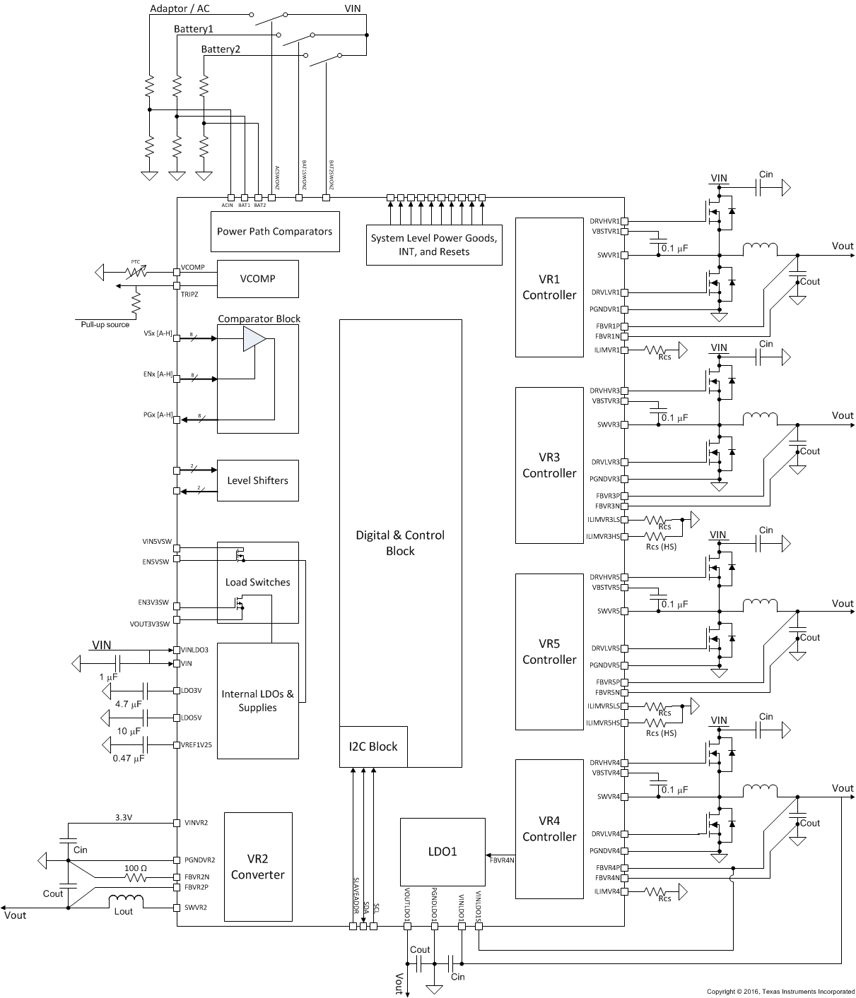 Figure 7-1 Simplifed General Block Diagram
7.2.1 Design Requirements
The TPS65083x requires decoupling caps on the supply pins. Refer to the Electrical Characteristics for recommended capacitance on these supplies.
The controllers, converter, LDO, and some other features can be adjusted to meet the application needs. The following describes how to design and adjust the external components to achieve desired performances.
7.2.2 Detailed Design Procedure
7.2.2.1 Controller Design Procedure
Designing the controller breaks down into several steps: designing the output filter, selecting the FETs, bootstrap capacitor, and input capacitors and setting the current limits.
Controllers VR1 and VR4 require VREG supply and capacitors. VREG should be connected to the 5-V LDO and a 1-µF, X5R, 20%, 10-V or similar capacitor should be used for decoupling.
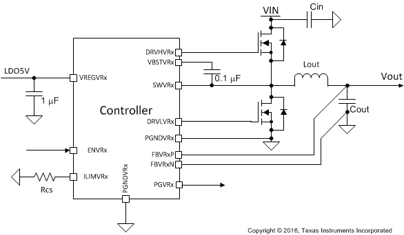 Figure 7-2 Controller Diagram
7.2.2.1.1 Selecting the Inductor
An inductor is required to be placed between the external FETs and the output capacitors. The inductor and output capacitors together make the double-pole which contributes towards stability. In addition, the inductor is directly responsible for the output ripple, efficiency, and transient performance. With an increase in inductance used the ripple current decreases which, typically increases efficiency. However, with an increase in inductance used, the transient performance decreases. Finally, the inductor selected has to be rated for appropriate saturation current, core losses, and DC resistance (DCR).
Use the equation below to calculate the recommended inductance for the controller. Let KIND be the ratio of ILripple to the IoutMAX. It is recommended that KIND is set to a value between 0.2 and 0.4.

With the chosen inductance value, the peak current for the inductor in steady state operation, ILmax, can be calculated using the equation below. The rated saturation current of the inductor must be higher than the ILmax current.

Following these equations the preferred inductor selected for the controllers are listed below in Table 7-1.
Table 7-1 Recommended Inductors
| MANUFACTURER | PART NUMBER | VALUE | SIZE | HEIGHT |
|---|---|---|---|---|
| Cyntec | PIME031B | 0.47 µH - 1 µH | 3.3 mm x 3.7 mm | 1.2 mm |
| Cyntec | PIMB041B | 0.33 µH - 2.2 µH | 4.45 mm x 4.75 mm | 1.2 mm |
| Cyntec | PIMB051B | 1 µH - 3.3 µH | 5.4 mm x 5.75 mm | 1.2 mm |
| Cyntec | PIME051E | 0.33 µH - 4.7 µH | 5.4 mm x 5.75 mm | 1.5 mm |
| Cyntec | PIMB051H | 0.47 µH - 4.7 µH | 5.4 mm x 5.75 mm | 1.8 mm |
| Cyntec | PIME061B | 0.56 µH - 3.3 µH | 6.8 mm x 7.3 mm | 1.2 mm |
| Cyntec | PIME061E | 0.33 µH - 4.7 µH | 6.8 mm x 7.3 mm | 1.5 mm |
| Cyntec | PIMB061H | 0.1 µH - 4.7 µH | 6.8 mm x 7.3 mm | 1.8 mm |
7.2.2.1.2 Selecting the Output Capacitors
Ceramic capacitors with low ESR values provide the lowest output voltage ripple and are recommended. The output capacitor requires either an X7R or X5R dielectric. Y5V and Z5U dielectric capacitors, aside from their wide variation in capacitance over temperature, become resistive at high frequencies.
At light load currents, the converter operates in Power Save Mode and the output voltage ripple is dependent on the output capacitor value and the PFM peak inductor current. Higher output capacitor values minimize the voltage ripple in PFM Mode. In order to achieve specified regulation performance and low output voltage ripple, the DC-bias characteristic of ceramic capacitors must be considered. The effective capacitance of ceramic capacitors drops with increasing DC bias voltage.
For the output capacitors of the DCDC controller the use of a small ceramic capacitors placed as close as possible to the inductor and the respective PGND pins of the IC is recommended. This solution typically, provides the smallest and lowest cost solution available for DCAP2 controllers.
7.2.2.1.3 Selecting the FETs
This controller is designed to drive NMOS FETs. Typically, the lower RDSon for the high and low side FETs the better but, be sure to size the FETs, inductor and output capacitors appropriately as the RDSon for the low side FET decreases, the minimum current limit increases. The Texas Instruments CSD87381P is recommended for the controllers.
7.2.2.1.4 Bootstrap Capacitor
To make sure that the internal high side gate drivers are supplied with a stable low noise supply voltage, a capacitor must be connected between the VBSTVRx pins and the respective SWVRx pins. Using ceramic capacitors with the value of 0.1 µF are recommended for the converters and the controllers, respectfully. For testing, a 0.1-µF, size 0402, 10-V capacitor was used for the controllers.
It is recommended to reserve a small resistor in series with the bootstrap capacitor in case the turn on / off of the FETs need to be slowed in order to reduce voltage ringing on the switch node. This is common practice for controller design.
7.2.2.1.5 Setting the Current Limits
The controller has a Valley Current Limit topology, also known as a Low Side Current Limit. This type of current limit works by limiting the current only when the low side FET is on. If the current being sourced by the low side FET is greater than the set low side current limit, ILS, the controller will hold the low side FET on and the high side off until the current through the low side FET decreases below the set ILS. Only if the current through the low side FET is less than the ILS will the low side FET be allowed to turn off and the high side FET to turn on.
A fast current increase is limited by the maximum on time for the high side FET. This forces the low side FET to turn on every period. Once the low side FET turns on, the Low Side Current Limit can control the FETs until the current decreases below the ILS. The maximum on time for the high side FET limits the current increase to maximum on time multiplied by the di/dt of the inductor until the low side FET is switched on.
IOCL is the average current when the valley current is consistently the ILS.
 Figure 7-3 IOCL Depiction
The low side current limit for the controllers is set by a resistor, RCS, at the ILIMx pin. A current, ITRIP, is sourced across the RCS to set the voltage for the current limit comparator. Use the equation below to determine the RCS resistor. It is recommended to set IOCL to 130% of IOUTmax and use a resistor with ±1% or less tolerance for best results. Since the current limit is when the inductor current is near its maximum it is recommended to use the saturation derating of the inductor when calculating the RCS.

There is a minimum and a maximum IOCL that can be achieved for the given parameters used in the equation above. To ensure that the RCS has been sized correctly, the following equation must be true across the application temperature range.

If the controller has high side current limit then, use Equation 5 to calculate the high side RCS resistor. The high side current limit must be set higher than the low side current limit. Again, since the current limit is when the inductor current is near its maximum it is recommended to use the saturation derating of the inductor when calculating the RCS.

7.2.2.1.6 Selecting the Input Capacitors
Because of the nature of the switching converter and controller with a pulsating input current, a low ESR input capacitor is required for best input voltage filtering and minimizing the interference with other circuits caused by high input voltage spikes. For the controller, 12 µF of input capacitance is recommended for most applications. To achieve the low ESR requirement, a ceramic capacitor is recommended. However, the voltage rating and DC bias characteristic of ceramic capacitors need to be considered. The input capacitor can be increased without any limit for better input voltage filtering. Be sure to size the ceramic capacitor to achieve the recommended input capacitance. A ceramic capacitor placed as close as possible to the respective VINx and PGNDx pins of the FETs is recommended.
The preferred capacitors for the controllers are two muRata GRM21BR61E106MA73: 10 μF, 0805, 25 V, ±20% or similar.
7.2.2.2 Converter Design Procedure
Designing the converter has only 2 steps: designing the output filter and selecting the input capacitors. The converter must be supplied by a 3.3-V source which can be provided by one of the TPS65083x controllers.
The converter requires VREG supply and capacitors. VREG should be connected to the 5-V LDO and a 1-µF, X5R, 20%, 10-V or similar capacitor should be used for decoupling.
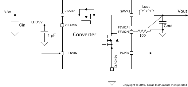 Figure 7-4 Converter Diagram
7.2.2.2.1 Selecting the Inductor
An inductor is required to be placed between the SWVRx and the output capacitors. The inductor and output capacitors together make the double-pole which contributes towards stability. In addition, the inductor is directly responsible for the output ripple, efficiency, and transient performance. With an increase in inductance used the ripple current decreases which, typically increases efficiency. However, with an increase in inductance used, the transient performance decreases. Finally, the inductor selected has to be rated for appropriate saturation current, core losses and DC resistance (DCR).
Use the equation below to calculate the recommended inductance for the controller. Let K IND be the ratio of I Lripple to the Iout MAX. It is recommended that K IND is set to a value between 0.2 and 0.4.

With the chosen inductance value, the peak current for the inductor in steady state operation, I - Lmax , can be calculated using the equation below. The rated saturation current of the inductor must be higher than the I Lmax current.

Following these equations the preferred inductors selected for the converter are listed below in Table 7-2.
Table 7-2 Recommended Inductors
| MANUFACTURER | PART NUMBER | VALUE | SIZE | HEIGHT |
|---|---|---|---|---|
| Cyntec | PIFE32251B-R68MS | 0.68 µH | 3.2 mm x 2.5 mm | 1.2 mm |
| Würth | 744383230068 | 0.68 µH | 2.5 mm x 2 mm | 1.0 mm |
7.2.2.2.2 Selecting the Output Capacitors
Ceramic capacitors with low ESR values provide the lowest output voltage ripple and are recommended. The output capacitor requires either an X7R or X5R dielectric. Y5V and Z5U dielectric capacitors, aside from their wide variation in capacitance over temperature, become resistive at high frequencies.
At light load currents, the converter operates in Power Save Mode and the output voltage ripple is dependent on the output capacitor value and the PFM peak inductor current. Higher output capacitor values minimize the voltage ripple in PFM Mode. In order to achieve specified regulation performance and low output voltage ripple, the DC-bias characteristic of ceramic capacitors must be considered. The effective capacitance of ceramic capacitors drops with increasing DC bias voltage.
For the output capacitors of the DCDC converters the use of a small ceramic capacitors placed as close as possible to the inductor and the respective PGND pins of the IC is recommended. If, for any reason, the application requires the use of large capacitors which can not be placed close to the IC, use a smaller ceramic capacitor in parallel to the large capacitor. The small capacitor should be placed as close as possible to the inductor and the respective PGND pins of the IC.
At the DCDC converters the recommended capacitor for use is the muRata GRM188R60J226MEAO: 22 µF, 0603, 6.3 V, ±20% or similar. This capacitor was selected to achieve the highest derated capacitance in a small 0603 package. If the selected output voltage is greater than 3.3 V then the muRata GRM21BR61A226ME44: 22 µF, 0805, 10 V, ±20%, or similar is recommended for use. This capacitor is recommended to maintain the actual capacitance as DC bias increases.
7.2.2.2.3 Selecting the Input Capacitors
Because of the nature of the switching converter and controller with a pulsating input current, a low ESR input capacitor is required for best input voltage filtering and minimizing the interference with other circuits caused by high input voltage spikes. For the controller, 12 µF of input capacitance is recommended for most applications. To achieve the low ESR requirement, a ceramic capacitor is recommended. However, the voltage rating and DC bias characteristic of ceramic capacitors need to be considered. The input capacitor can be increased without any limit for better input voltage filtering. Be sure to size the ceramic capacitor to achieve the recommended input capacitance. A ceramic capacitor placed as close as possible to the respective VINx and PGNDx pins of the IC is recommended.
The preferred capacitors for the controllers are two muRata GRM21BR61E106MA73: 10 μF, 0805, 25 V, ±20% or similar.
7.2.2.3 LDO Design Procedure
The LDO must handle the fast load transients from the DDR memory for termination. Therefore, it is important to maintain a high amount of capacitance with low ESR on the LDO outputs and inputs. Ceramic capacitors are ideal for this. Below is the recommended capacitors.
The preferred output capacitor for the LDO is muRata GRM188R60J476M: 47 μF, 0603, 6.3 V, ±20% or similar.
The preferred input capacitor for the LDO is muRata GRM155R60J106ME44: 10 μF, 0402, 6.3 V, ±20% or similar.
7.2.2.4 Board Temperature Monitoring Design Procedure
Board temperature monitoring requires only 1 thermistor if only 1 sense point is desired. It can be scaled by adding as many thermistors as sense points desired. Simply connect a PTC thermistor that has an exponential coefficient curve from the VCOMP pin to GND and a pull up to desired voltage source on the TRIPZ pin. Place thermistor where desired. If multiple sense points are desired string the thermistors together in a series connection while placing the thermistors where desired.
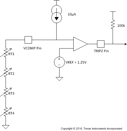 Figure 7-5 Board Temperature Monitoring Circuit Example
The thermistors should have low room and mid temperature resistances in the range of 1 kΩ to 10 kΩ. The hot point resistance should be roughly 10x mid temperature resistance in the range of 100 kΩ to 200 kΩ. There is an internal 10-µA current source that provides a voltage across the thermistors. Once this voltage exceeds the comparator threshold of 1.25 V the TRIPZ pin switches to LOW indicating a HOT board temperature. Therefore, the resistance required for HOT board temperature is 125 kΩ. Select thermistors that align this resistance with the desired HOT temperature setpoint.
The recommended thermistors for this feature is the muRata PRF15BG102RB6RC.
7.2.2.5 Power Path Design Procedure
The TPS65083x has power path comparators and outputs to control the power path switches. Simply connect a voltage divider to the adaptor and batteries to set the threshold to the desired value. The outputs of the comparators require a pull up since they are open-drain outputs. In-order for the power path comparators to work without VIN supplied connect the VINPP to the power rails that are being monitored by using a diode to select the highest voltage among the sources.
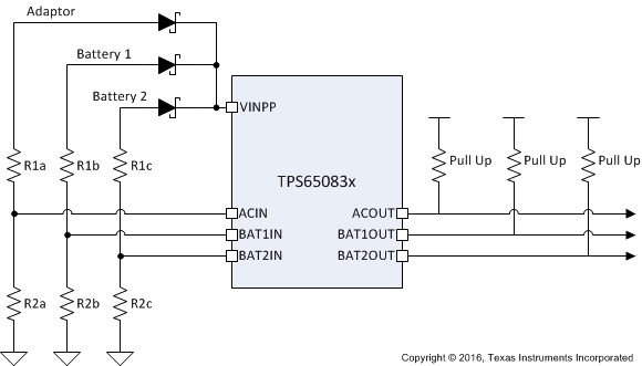 Figure 7-6 Power Path Comparators and VINPP Supply
Example:
Desired is to measure a battery and an adaptor to decide when to switch over from battery to adaptor. The voltages desired for thresholds are 9 V and 6 V respectively. Using Equation 8 the resistors required to set the 9-V threshold are R1a = and R2a = . The resistors required to set the 6-V threshold are R1b = and R2b = .

7.2.3 Application Performance Curves
Table 7-3 Application Curves Overview
| TYPE | DESCRIPTION AND ASSUMPTIONS | FIGURE NUMBER |
|---|---|---|
| Efficiency VR1 | Using CSD87381P FET Block, PIME051H-1R0MS, 3 x GRM31CR60G227ME11 + 1 x GRM21BR60J107M, NDVCZ = HIGH, Vout = 1 V |
Figure 7-7 |
| Efficiency VR2 | Using PIFE32251B-R68MS, 4 x ZRB18AR60G476ME01, NDVCZ = HIGH, Vout = 1.8 V |
Figure 7-8 |
| Efficiency VR3 | Using CSD87381P FET Block, PIMB061H-1R5MS, 3 x GRM21BR60J107M , NDVCZ = HIGH, Vout = 3.3 V |
Figure 7-9 |
| Efficiency VR4 | Using CSD87381P FET Block, PIME051H-1R0MS, 2 x GRM31CR60G227ME11 + 1 x GRM21BR60J107M, NDVCZ = HIGH, Vout = 1.2 V |
Figure 7-10 |
| Efficiency VR5 | Using CSD87381P FET Block, PIMB051H-3R3MS, 11 x GRM21BR61A476ME15, NDVCZ = HIGH, Vout = 5 V |
Figure 7-11 |
spacing
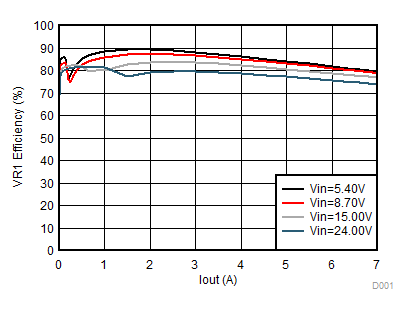 Figure 7-7 Typical Efficiency for VR1
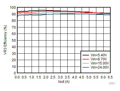 Figure 7-9 Typical Efficiency for VR3
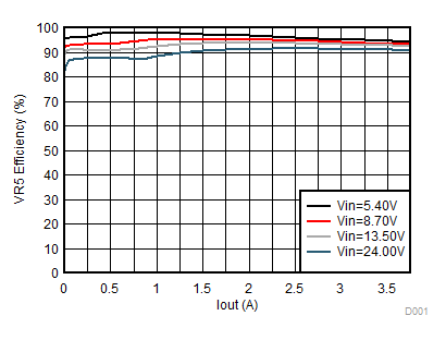 Figure 7-11 Typical Efficiency for VR5
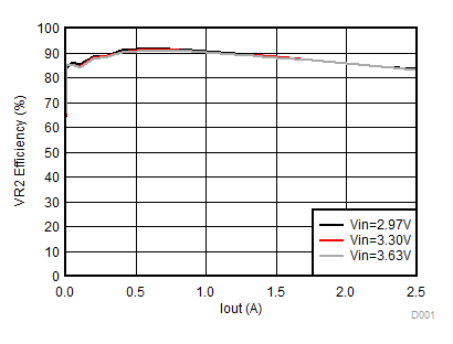 Figure 7-8 Typical Efficiency for VR2
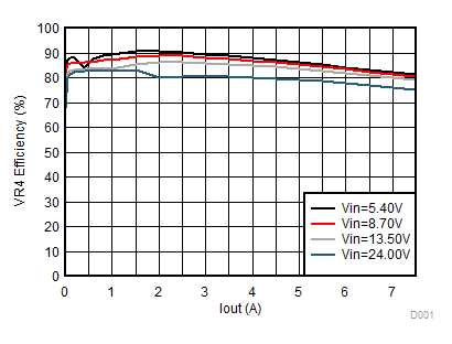 Figure 7-10 Typical Efficiency for VR4
7.2.4 Specific Application - TPS650830 Powering the Intel SkyLake and Kabylake Platform Volume Configuration
Volume configuration is the lowest cost and smallest solution for SkyLake and Kabylake power. It combines multiple same voltage rails into one rail reducing cost and size. Load switches are utilized to separate the rails and power the system with correct sequencing. The PMIC controls these load switches with the power good comparators. The TPS65083x also supports Premium configurations, see TPS650831 and TPS650832 or literature numbers: SLVSCS5 and SLVSCS6.
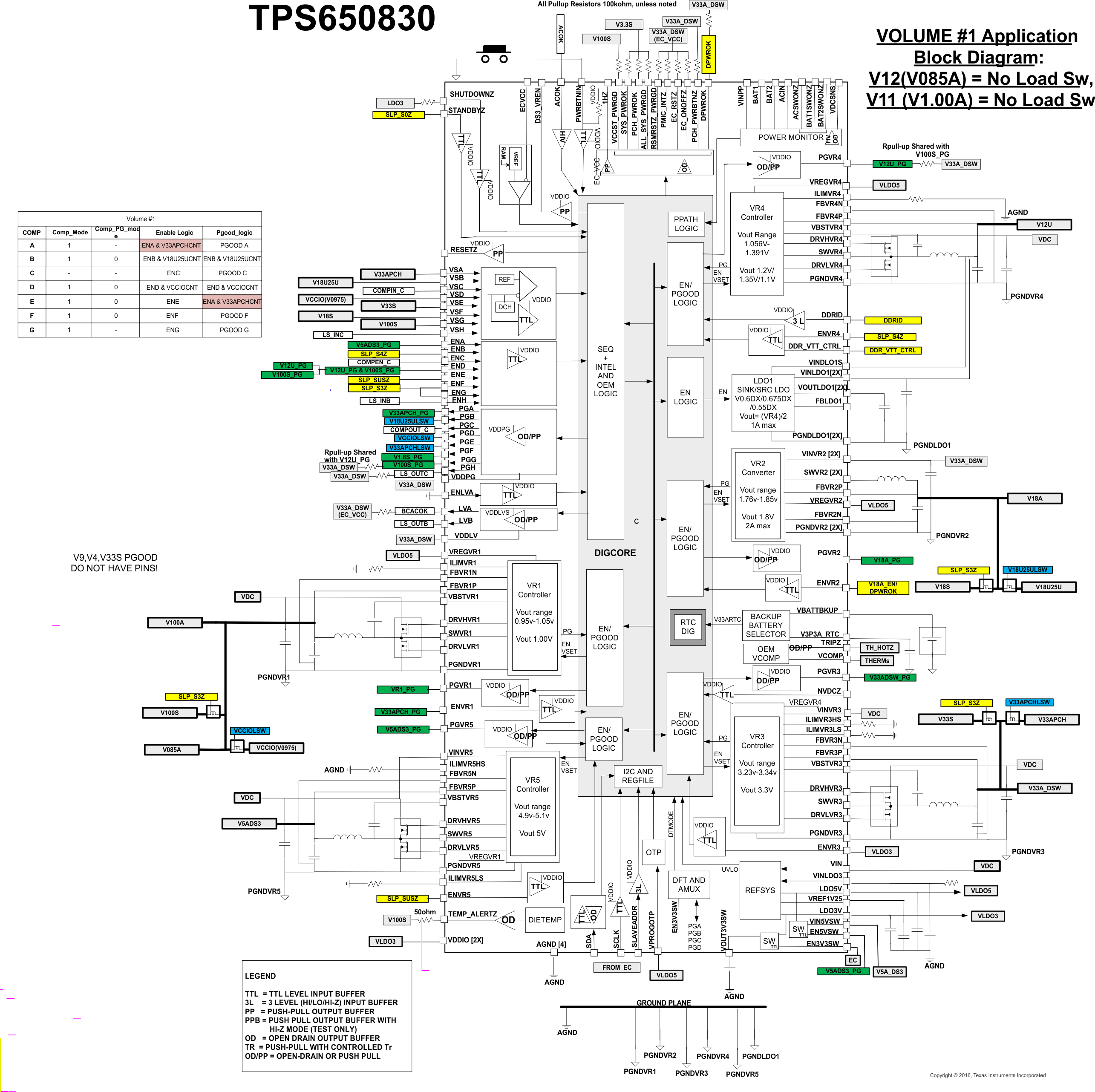 Figure 7-12 TPS650830 Volume Application Diagram
7.2.4.1 Design Requirements
The deisgn requirements are set by the Intel SkyLake and Kabylake Platform. Below are the requirements of the power supply system. This procedure assumes the system is a 2S NVDC system but, the TPS65083x supports 3S NVDC, as well as non-NVDC systems. 2S NVDC system has an input voltage range of 5.4 V to 8.7 V.
- There must be 9 separate voltage rails:
- V5A_DS3 - 5 V, IMAX = 3.5 A
- V3.3A_DSW - 3.3 V, IMAX = 3.5 A
- V3.3A_PCH - 3.3 V, IMAX = 3 A
- V1.00A - 1.0 V, IMAX = 4.9 A
- VCCIO - 1.0 V, IMAX = 2.9 A
- V1.8A - 1.8 V, IMAX = 1 A
- V1.8U - 1.8 V, IMAX = 1 A
- VDDQ - 1.2 V, IMAX = 7.5 A
- VTT - 0.6 V, IMAX = ±1A
- All rails must have maximum tolerance of ±5% of the nominal voltage at all times with load transients.
- Load Transients are defined as 0% to 70%, 70% to 0%, 30% to 100% and 100% to 30% load current steps relative of the IMAX current defined for each rail.
- Maximum height of components = 1.8 mm.
- Sequence in the order below:
- V3.3A_DSW with VIN supplied
- V1.8A with VIN supplied
- V5A_DS3 with SLP_SUS# transition to HIGH
- V3.3A_PCH with SLP_SUS# transition to HIGH
- V1.00A with SLP_SUS# transition to HIGH
- VDDQ with SLP_S4# transition to HIGH
- V1.8U with SLP_S4# transition to HIGH
- VCCIO with SLP_S3# transition to HIGH
- VTT with DDR_VTT_CTRL / SLP_S0# transition to HIGH
7.2.4.2 Detailed Design Procedure
The TPS650830 supplies 6 voltage rails and controls 3 load switches to meet the sequence order for the V3.3A_PCH, V1.8U, and VCCIO rails.
- VR1 supplies the V1.00A rail and the VCCIO rail with a load switch.
- VR2 supplies the V1.8A rail and the V1.8U rail with a load switch.
- VR3 supplies the V3.3A_DSW rail and the V3.3A_PCH rail with a load switch.
- VR4 supplies the VDDQ rail and the VINLDO1 for termination.
- VR5 supplies the V5A_DS3 rail.
- VLDO1 supplies the VTT rail.
To meet the sequencing requirement the power goods of the VRs and PG comparators are feed back into the enables for the VRs and comparators. The 5 external control signals SLP_SUS#, _S4#, _S3#, _S0#, and DDR_VTT_CTRL are responsible for transitioning the system from sleep state to sleep state and the reverse sequencing.
Since, the requirements are for a 2S NVDC system the NVDCZ pin should be tied LOW.
7.2.4.2.1 Output Inductance and Capacitance
Following the recommend design procedure in Section 7.2.2 will yield output inductance and capacitance similar to Table 7-4.
Table 7-4 SkyLake and Kabylake Volume Configuration Output L and C
| VRx | OUTPUT INDUCTANCE | MINIMUM OUTPUT CAPACITANCE | RECOMMENDED OUTPUT CAPACITORS | CAPACITOR MANUFACTURER |
|---|---|---|---|---|
| VR1 | 0.56 µH | 160 µF | 1 x GRM31CR60G227ME11 and 1 x ZRB18AR60G476ME01 |
muRata |
| VR2 | 0.68 µH | 47 µF | 4 x ZRB18AR60G476ME01 | muRata |
| VR3 | 1 µH | 87 µF | 2 x GRM31CR60G227ME11 | muRata |
| VR4 | 0.56 µH | 117 µF | 1 x GRM31CR60G227ME11 | muRata |
| VR5 | 2.2 µH | 76 µF | 8 x GRM21BR61A476ME15 | muRata |
7.2.4.3 Application Performance Curves
Table 7-5 Application Curves Overview
| TYPE | DESCRIPTION AND ASSUMPTIONS | FIGURE NUMBER |
|---|---|---|
| Efficiency VR1 | Using CSD87381P FET Block, PIMB051H-0R56M, 1 x GRM31CR60G227ME11 + 1 x ZRB18AR60G476ME01, NDVCZ = LOW, Vout = 1 V |
Figure 7-13 |
| Efficiency VR2 | Using PIFE32251B-R68MS, 4 x ZRB18AR60G476ME01, NDVCZ = LOW, Vout = 1.8 V |
Figure 7-14 |
| Efficiency VR3 | Using CSD87381P FET Block, PIME051H-1R0MS, 2 x GRM31CR60G227ME11, NDVCZ = LOW, Vout = 3.3 V |
Figure 7-15 |
| Efficiency VR4 | Using CSD87381P FET Block, PIMB051H-0R56M, 1 x GRM31CR60G227ME11, NDVCZ = LOW, Vout = 1.2 V |
Figure 7-16 |
| Efficiency VR5 | Using CSD87381P FET Block, PIME051B-2R2MS, 8 x GRM21BR61A476ME15, NDVCZ = LOW, Vout = 5 V |
Figure 7-17 |
space
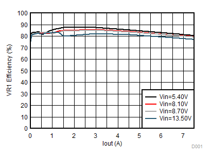 Figure 7-13 Typical Efficiency for VR1
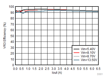 Figure 7-15 Typical Efficiency for VR3
 Figure 7-17 Typical Efficiency for VR5
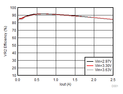 Figure 7-14 Typical Efficiency for VR2
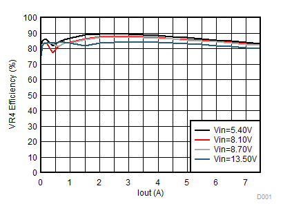 Figure 7-16 Typical Efficiency for VR4
7.3 System Example
Below is a diagram of the SkyLake and Kabylake Platform System Power Delivery. The PMIC is flexible and adjusts well across SkyLake and Kabylake platforms.
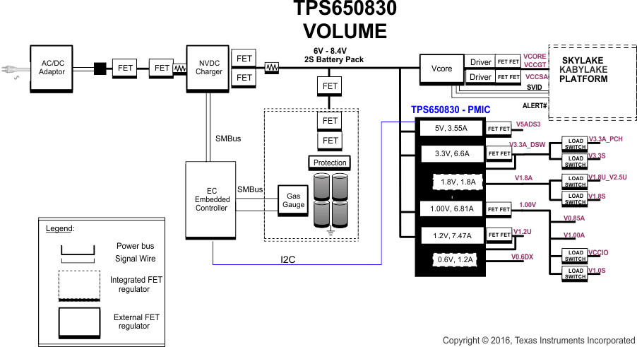 Figure 7-18 TPS650830 Volume Simplified System Power Configuration Diagram
7.4 Do's and Don'ts
- Always either float or connect the VINPP to the same voltage as VIN. Never ground VINPP.
- If not using a voltage regulator connect the enable to ground and float the output.