SLVSCF4A December 2014 – July 2016 TPS650830
PRODUCTION DATA.
- 1 Device Overview
- 2 Revision History
- 3 Device Options
- 4 Pin Configuration and Functions
- 5 Specifications
-
6 Detailed Description
- 6.1 Overview
- 6.2 Functional Block Diagram
- 6.3
Feature Description
- 6.3.1 Voltage Regulator Assignment and Powergood Comparator Logic Assignment (External Voltage Regulator or Load Switch) for Skylake and Kabylake Platform
- 6.3.2 Generic Powergood Window Comparator with Open-Drain Output
- 6.3.3 Powergood Window Comparator
- 6.3.4 3.3-V LDO and 3V3SW Load Switch
- 6.3.5 5-V LDO and 5VSW Load Switch
- 6.3.6 RTC Selector and 3.1-V LDO
- 6.3.7 Power Path Comparators
- 6.3.8 UVLO Comparators
- 6.3.9 Temperature Comparator
- 6.3.10 Low Power Mode (LPM) / Connected Standby / Instant Go of VRs
- 6.3.11 Enable and Powergood of VRs
- 6.3.12 VR4 VDDQ and LDO1 VTT Enabling
- 6.3.13
Converters
- 6.3.13.1 Power Save Mode
- 6.3.13.2 Voltage Regulator Startup
- 6.3.13.3 Powergood, Power Fault, and Emergency Power Shutdown
- 6.3.13.4 Current Limit
- 6.3.13.5 Output Discharge Feature
- 6.3.13.6 Output Voltage Control
- 6.3.13.7 Converter Low Power Mode Operation
- 6.3.13.8 Controller Low Power Mode Operation
- 6.3.13.9 Controller Internal Ramp Comparator
- 6.3.13.10 Undervoltage Lockout
- 6.3.14 Coincell Selector
- 6.4 Device Functional Modes
- 6.5 Programming
- 6.6
Register Map
- 6.6.1
Registers
- 6.6.1.1 VENDORID Register (address = 0x00) [reset = 00100010]
- 6.6.1.2 REVID Register (address = 0x01) [reset = 00000000]
- 6.6.1.3 IRQLVL1 Register (address = 0x02) [reset = 00000000]
- 6.6.1.4 PWRSRCINT Register (address = 0x04) [reset = 00000000]
- 6.6.1.5 PMUINT Register (address = 0x05) [reset = 00000000]
- 6.6.1.6 RESETIRQ1 Register (address = 0x08) [reset = 00000000]
- 6.6.1.7 RESETIRQ2 Register (address = 0x09) [reset = 00000000]
- 6.6.1.8 MPMUINT Register (address = 0x0B) [reset = 00010100]
- 6.6.1.9 MPWRSRCINT Register (address = 0x0C) [reset = 01111000]
- 6.6.1.10 RESETIRQ1MASK Register (address = 0x11) [reset = 00110000]
- 6.6.1.11 RESETIRQ2MASK Register (address = 0x12) [reset = 00000010]
- 6.6.1.12 IRQLVL1msK Register (address = 0x13) [reset = 10100101]
- 6.6.1.13 PBCONFIG Register (address = 0x14) [reset = 00011111]
- 6.6.1.14 PBSTATUS Register (address = 0x15) [reset = 00000000]
- 6.6.1.15 PWRSTAT1 Register (address = 0x16) [reset = 00000000]
- 6.6.1.16 PWRSTAT2 Register (address = 0x17) [reset = 00000000]
- 6.6.1.17 PGMASK1 Register (address = 0x18) [reset = 00000000]
- 6.6.1.18 PGMASK2 Register (address = 0x19) [reset = 00000000]
- 6.6.1.19 VCCIOCNT Register (address = 0x30) [reset = 00001010]
- 6.6.1.20 V5ADS3CNT Register (address = 0x31) [reset = 00101010]
- 6.6.1.21 V33ADSWCNT Register (address = 0x32) [reset = 00101010]
- 6.6.1.22 V33APCHCNT Register (address = 0x33) [reset = 00001010]
- 6.6.1.23 V18ACNT Register (address = 0x34) [reset = 00101010]
- 6.6.1.24 V18U25UCNT Register (address = 0x35) [reset = 00001010]
- 6.6.1.25 V1P2UCNT Register (address = 0x36) [reset = 00111010]
- 6.6.1.26 V100ACNT Register (address = 0x37) [reset = 00011010]
- 6.6.1.27 V085ACNT Register (address = 0x38) [reset = 00101010]
- 6.6.1.28 VRMODECTRL Register (address = 0x3B) [reset = 00111111]
- 6.6.1.29 DISCHCNT1 Register (address = 0x3C) [reset = 00000000]
- 6.6.1.30 DISCHCNT2 Register (address = 0x3D) [reset = 00000000]
- 6.6.1.31 DISCHCNT3 Register (address = 0x3E) [reset = 00000000]
- 6.6.1.32 DISCHCNT4 Register (address = 0x3F) [reset = 00000000]
- 6.6.1.33 PWRGDCNT1 Register (address = 0x40) [reset = 01011111 ]
- 6.6.1.34 VREN Register (address = 0x41) [reset = 00000000]
- 6.6.1.35 REGLOCK Register (address = 0x42) [reset = 00000000]
- 6.6.1.36 VRENPINMASK Register (address = 0x43) [reset = 00000000]
- 6.6.1.37 RSTCTRL Register (address = 0x48) [reset = 00011100]
- 6.6.1.38 SDWNCTRL Register (address = 0x49) [reset = 00000000]
- 6.6.1.39 VDLMTCRT Register (address = 0x51) [reset = 00000101]
- 6.6.1.40 ACOKDBDM Register (address = 0x69) [reset = 00001111]
- 6.6.1.41 LOWBATTDET Register (address = 0x6A) [reset = 11111000]
- 6.6.1.42 SPWRSRCINT Register (address = 0x6F) [reset = 00000000]
- 6.6.1.43 CLKCTRL1 Register (address = 0xD0) [reset = 00000000]
- 6.6.1.44 COMPA_REF Register (address = 0xDD) [reset = 00000000]
- 6.6.1.45 COMPB_REF Register (address = 0xDE) [reset = 00000000]
- 6.6.1.46 COMPC_REF Register (address = 0xDF) [reset = 00000000]
- 6.6.1.47 COMPD_REF Register (address = 0xE0) [reset = 00000000]
- 6.6.1.48 COMPE_REF Register (address = 0xE1) [reset = 00000000]
- 6.6.1.49 COMPF_REF Register (address = 0xE2) [reset = 00000000]
- 6.6.1.50 COMPG_REF Register (address = 0xE3) [reset = 00000000]
- 6.6.1.51 COMPH_REF Register (address = 0xE4) [reset = 00000000]
- 6.6.1.52 PWFAULT_MASK1 Register (address = 0xE5) [reset = 00000000]
- 6.6.1.53 PWFAULT_MASK2 Register (address = 0xE6) [reset = 00000000]
- 6.6.1.54 PGOOD_STAT1 Register (address = 0xE7) [reset = 00000000]
- 6.6.1.55 PGOOD_STAT2 Register (address = 0xE8) [reset = 00000000]
- 6.6.1.56 MISC_BITS Register (address = 0xE9) [reset = 00010000]
- 6.6.1.57 STDBY_CTRL Register (address = 0xEA) [reset = 11111110]
- 6.6.1.58 TEMPCRIT Register (address = 0xEB) [reset = 00000000]
- 6.6.1.59 TEMPHOT Register (address = 0xEC) [reset = 00000000]
- 6.6.1.60 VREN_PIN_OVR Register (address = 0xEE) [reset = 00000000]
- 6.6.1
Registers
-
7 Application and Implementation
- 7.1 Application Information
- 7.2
Typical Application
- 7.2.1 Design Requirements
- 7.2.2 Detailed Design Procedure
- 7.2.3 Application Performance Curves
- 7.2.4 Specific Application - TPS650830 Powering the Intel SkyLake and Kabylake Platform Volume Configuration
- 7.3 System Example
- 7.4 Do's and Don'ts
- 8 Power Supply Recommendations
- 9 Layout
- 10Device and Documentation Support
- 11Mechanical, Packaging, and Orderable Information
Package Options
Mechanical Data (Package|Pins)
Thermal pad, mechanical data (Package|Pins)
Orderable Information
5 Specifications
5.1 Absolute Maximum Ratings
over operating free-air temperature range (unless otherwise noted)(1)(1) Stresses beyond those listed under Absolute Maximum Ratings may cause permanent damage to the device. These are stress ratings only, which do not imply functional operation of the device at these or any other conditions beyond those indicated under Recommended Operating Conditions. Exposure to absolute-maximum-rated conditions for extended periods may affect device reliability.
5.2 ESD Ratings
| VALUE | UNIT | |||
|---|---|---|---|---|
| V(ESD) | Electrostatic discharge | Human body model (HBM), per ANSI/ESDA/JEDEC JS-001 (1) | 1500 | V |
| Charged device model (CDM), per JEDEC specification JESD22-C101 (2) | 500 | V | ||
(1) JEDEC document JEP155 states that 500-V HBM allows safe manufacturing with a standard ESD control process.
(2) JEDEC document JEP157 states that 250-V CDM allows safe manufacturing with a standard ESD control process.
5.3 Recommended Operating Conditions
over operating free-air temperature range (unless otherwise noted)5.4 Thermal Information
| THERMAL METRIC (1) | TPS650830 | UNIT | ||
|---|---|---|---|---|
| ZAJ (NFBGA) | ZCG (NFBGA) | |||
| 168 PINS | 159 PINS | |||
| RθJA | Junction-to-ambient thermal resistance | 37.7 | 34.7 | °C/W |
| RθJC(top) | Junction-to-case (top) thermal resistance | 15.1 | 15.1 | °C/W |
| RθJB | Junction-to-board thermal resistance | 11.8 | 13.7 | °C/W |
| ψJT | Junction-to-top characterization parameter | 0.3 | 0.3 | °C/W |
| ψJB | Junction-to-board characterization parameter | 11.7 | 13.8 | °C/W |
| RθJC(bot) | Junction-to-case (bottom) thermal resistance | N/A | N/A | °C/W |
(1) For more information about traditional and new thermal metrics, see Semiconductor and IC Package Thermal Metrics application report.
5.5 Electrical Characteristics
Over recommended free-air temperature range and over recommended input voltage range (typical at an ambient temperature range of 25°C) (unless otherwise noted)| PARAMETER | TEST CONDITIONS | MIN | TYP | MAX | UNIT | ||
|---|---|---|---|---|---|---|---|
| CONTROL | |||||||
| CONTROL - SYSTEM | |||||||
| VIN Parametric | System input voltage | Parametric and functional | 5.4 | 7.4 | 21 | V | |
| VIN Functional | System input voltage | Functional | 5.4 | 7.4 | 24 | V | |
| IQ | System quiescent current (includes IDDQ for LDO5V, LDO3V, and VREF1.25V, all registers are default setting) | Measured at VIN = 7.4 V | 95 | 150 | μA | ||
| VUVLO_5V_Main | System under voltage lockout threshold - All IC functionality including 5VLDO, except LDO3V and internal refsys | VVIN voltage decreasing - measured at VIN (falling edge) | 4.95 | 5.1 | 5.25 | V | |
| VHys_5V_Main | System under voltage lockout threshold hysteresis | VVIN voltage increasing - measured at VIN | 200 | mV | |||
| CONTROL - INTERNAL REFERENCES | |||||||
| VO(VLDO5) | LDO5V output | VIN = 5.4 V - 21 V, 10-mA load | 4.9 | 5.0 | 5.1 | V | |
| Line regulation VO(LDO5V) | Line regulation for regulator over operating voltage range | VIN = 5.4 V to 21 V, Measured as (ΔVO(LDO5V)/VO(LDO5V)) over this operating range with 40-mA load current. measured at LDO5V pin with respect to AGND pin | 0.5% | ||||
| Load regulation VO(LDO5V) | Load regulation for regulator over operating current range | VIN = 5.4 V - 21 V Measured as (ΔVO(LDO5V)/VO(LDO5V)) over this operating range with 10-mA to 100-mA load current. measured at LDO5V pin with respect to AGND pin | 2% | ||||
| ISC (LDO5V) | Over current protection | Measured at 90% of the regulation voltage | 115 | mA | |||
| CO (LDO5V) | External output capacitance range after derating | Actual capacitance after derating. ex: 2.7-µF capacitance, then use a 4.7-µF capacitor with 60% deratingat 5 V. | 2.7 | 4.7 | 10 | μF | |
| VO(VREF1V25) | VREF1V25 output - Internal buffered bandgap output | See below for output capacitance. measured at VREF1V25 pin with respect to AGND pin | 1.244 | 1.25 | 1.256 | V | |
| CO (VREF1V25) | External output capacitance range after derating | Actual capacitance after derating. ex: 0.27-µF capacitance, then use a 0.47-µF capacitor with 60% derating at 1.25 V | 0.2 | 1.0 | μF | ||
| VI(LDO3V) | LDO3V input | Parametric and functional | 5.4 | 7.4 | 21 | V | |
| VI(LDO3V) | LDO3V input | Functional | 3.45 | 7.4 | 24 | V | |
| VO(LDO3V) | LDO3V output | VIN = 7.4 V, 1-mA load | 3.267 | 3.3 | 3.333 | V | |
| IO (LDO3V) | Output current | Maximum current for external user is limited 40 mA | 40 | mA | |||
| ISC (LDO3V) | Output circuit current limit | Measured at 90% of the regulation voltage | 75 | mA | |||
| Line regulation VO(LDO3V) | Line regulation for regulator over operating voltage range | VIN = 5.4 V to 21 V, Measured as (ΔVO(LDO3V)/VO(LDO3V)) over the operating range with 20-mA load current. measured at LDO3V pin with respect to AGND pin | 0.5% | ||||
| Load regulation VO(LDO3V) | Load regulation for regulator over operating current range | VIN = 7.4 Measured as (ΔVO(LDO3V)/VO(LDO3V)) over this operating range with 0-mA to 50-mA load current. measured at LDO3V pin with respect to AGND pin | 0.5% | ||||
| CO (LDO3V) | External output capacitance range after derating | Actual capacitance after derating. ex: 2.7-µF capacitance, then use a 4.7-µF capacitor with 60% deratingat 3.3 V. | 2.2 | 4.7 | 10 | μF | |
| TR (LDO3V) | Rise time | Measured from 5% to 95% of the output voltage with 2.2 μF | 300 | 450 | μs | ||
| CONTROL - INPUT/ OUTPUT BUFFERS | |||||||
| CONTROL - DDR_VTT_CTRL (Intel external connection DDR_VTT_CTRL) - 1 V logic, tolerates 3 V | |||||||
| VIL_DDR_VTT_CTRL | DDR_VTT_CTRL input low voltage | Input low voltage threshold | 0.49 | V | |||
| VIH_DDR_VTT_CTRL | DDR_VTT_CTRL input high voltage | Input high voltage threshold | 0.61 | V | |||
| VHYST_DDR_VTT_CTRL | DDR_VTT_CTRL hysteresis voltage | Hysteresis voltage | 70 | mV | |||
| Ileakage_DDR_VTT_CTRL | DDR_VTT_CTRL input current | Input current, Clamped to 1.0 V | 0.01 | 0.2 | μA | ||
| CONTROL - INPUT TTL BUFFERS (ALL INPUT PINS), (DEFAULT: SHUTDOWNZ, STANDBYZ, ENLVA, EN3V3SW, EN5VSW, ENVR1, ENVR2, ENVR3, ENVR4, ENVR5, ENA. ENB, ENC, END, ENE, ENF, ENG, ENH), (OPTIONAL: VSA, VSB, VSC, VSD, VSE, VSF, VSG, VSH, ENLVA) | |||||||
| VIL_INPUTS | Input low voltage | 0.4 | V | ||||
| VIH_INPUTS | Input high voltage | 1.2 | V | ||||
| VHYST_INPUTS | Hysteresis voltage | 300 | mV | ||||
| Ileakage_INPUTS | Input current | Clamped on 3.3 V | 0.01 | 0.3 | μA | ||
| VIL_PWRBTNZ | Input low voltage for PWRBTNZ | 0.4 | V | ||||
| VIH_PWRBTNZ | Input high voltage for PWRBTNZ | Internal 5-kΩ pull-up resistor between PWRBTNZ pin and VDDIO | 1.6 | V | |||
| VHYST_PWRBTNZ | Hysteresis voltage for PWRBTNZ | 580 | mV | ||||
| IOutput_PWRBTNZ | Output current for PWRBTNZ when power button is pressed to close and pulling PWRBTNZ to GND. | PWRBTNZ = GND, Internal 5-kΩ pull-up resistor between PWRBTNZ pin and VDDIO | 660 | 790 | μA | ||
| TEC_ONOFFZ_Debouinc_0e | EC_ONOFFZ_Debounce time, 0 setting | Time set to 0 ms, Measured from 0.5% PWBTNZ rising to 5% of the EC_ONOFFZ output | 0 | ms | |||
| TEC_ONOFFZ_Debouinc_30e | EC_ONOFFZ_Debounce time, 30 ms setting | Time set to 30 ms, Measured from 0.5% PWBTNZ rising to 5% of the EC_ONOFFZ output | 30 | ms | |||
| CONTROL - VDDIO DOMAIN PUSH-PULL OUTPUTS, (RESETZ, 1HZ, DS3_VREN), (Optional: PGVR1, PGVR2, PGVR3, PGVR4, PGVR5) | |||||||
| VPP | Pull-up output voltage supply | Pulled-Up to VDDIO pin which should by tied to LDO3V pin = 3.3 V | VDDIO | V | |||
| VOL_PP | Low level output voltage | IOL = 3 mA | 0.6 | V | |||
| VOH_PP | High level output voltage | IOH = 3 mA | VDDIO - 0.6 | V | |||
| CONTROL - VDDPG DOMAIN PUSH-PULL OUTPUTS, (Optional: PGA, PGB, PGC, PGD, PGE, PGF, PGG, PGH) | |||||||
| VPP | Pull-up output voltage supply | Pulled-Up to VDDPG pin | VDDPG | V | |||
| VOL_PP | Low level output voltage | IOL = 3 mA | 0.6 | V | |||
| VOH_PP | High level output voltage | IOH = 3 mA | VDDPG - 0.6 | V | |||
| CONTROL - VDDLV DOMAIN PUSH-PULL OUTPUTS (Optional: LVA, LVB) | |||||||
| VPP_VDDLV | LV pull-up output voltage supply | Pulled up to VDDLV pin | VDDLV | V | |||
| VOL_PP_LV | LV low level output voltage | IOL = 3 mA | 0.6 | V | |||
| VOH_PP_LV | LV high level output voltage | IOH = 3 mA | VDDLV - 0.6 | V | |||
| CONTROL - GENERAL OPEN-DRAIN OUTPUTS, (ACSWONZ, BAT1SWONZ, BAT2SWONZ, VCCST_PWRGD, SYS_PWROK, PCH_PWROK, RSMRSTZ_PWRGD, ALL_SYS_PWRGD, PMIV_INTZ, EC_RSTZ, PCH_PWRBTNZ, EC_ONOFFZ, DPWROK) (Optional: PGA, PGB, PGC, PGD, PGE, PGF, PGG, PGH, PGVR1, PGVR2, PGVR3, PGVR4, PGVR5, LVA, LVB) | |||||||
| VOL_OD1 | OD- output voltage | IOL = 2 mA | 0.4 | V | |||
| ILK_OD1 | OD leakage current | V(PIN) = 3.3 V | 0.45 | μA | |||
| CONTROL - OPEN-DRAIN OUTPUT (TEMP_ALERT) | |||||||
| VOL_OD | Open-drain low level output voltage | IOL = 15 mA, with 75-Ω pull-up resistor to 1 V | 0.165 | V | |||
| ILK_OD | Open-drain leakage current | V(PIN) = 3.3 V, with 75-Ω pull-up resistor to 1 V | 0.35 | μA | |||
| CONTROL - TRISTATE INPUT BUFFER (SLAVEADDR, DDRID) | |||||||
| VIL_TRISTATE | Low level input voltage | IOL = 6 μA | 0.33 | V | |||
| VIH_TRISTATE | High level input voltage | IOH = 6 μA | 1.8 | V | |||
| ITRISTATE | ITRISTATE current | Maximum allowable current in or out of pin when floating to maintain FLOAT logic state | -0.650 | 0.675 | μA | ||
| ITRISTATE_TOTAL_PIN_GND | Total current drawn when pin connected to GND | VINLDO3 current when TRISTATE pin = GND | 6 | μA | |||
| ITRISTATE_TOTAL_PIN_3.3V | Total current drawn when pin connected to 3.3 V | VINLDO3 current when TRISTATE pin = LDO3V = 3.3 V | 6 | μA | |||
| ITRISTATE_TOTAL_PIN_FLOAT | Total current drawn when pin Floating | VINLDO3 current when TRISTATE pin = Floating | 4.5 | μA | |||
| CONTROL - VSA, VSB, VSC, VSD, VSE, VSF, VSG, VSH (EXTERNAL VR and EXTERNAL LOADSWITCH POWERGOOD COMPARATORS) | |||||||
| VSx input voltage range | When VSx configured as voltage sense input | 0.7 | 1.8 | 5 | V | ||
| VSx input leakage current | When VSx configured as voltage sense input, VSx = 5.7 V | 0 | 9 | μA | |||
| Powergood exit threshold high VSx | VSx rising out of powergood. When VSx configured as voltage sense input and powergood window comparator. | 106% | 108% | 110% | |||
| Powergood threshold high VSx hysteresis | VSx falling into powergood. When VSx configured as voltage sense input and powergood window comparator. | -3% | |||||
| Powergood exit threshold low VSx | VSx falling out of powergood. When VSx configured as voltage sense input and powergood window comparator. | 90% | 92% | 94% | |||
| Powergood threshold low VSx hystersis | VSx rising into powergood. When VSx configured as voltage sense input and powergood window comparator. | 3% | |||||
| TVSx_POWERGOOD_DEGLITCH | Powergood deglitch time for both rising and falling edges | VSx voltage must cross powergood threshold and stay for at least this time to change powergood output state.Measured from VSx into or out of powergood threshold, until PGx toggles, for both rising and falling edges. | 27 | 30 | 33 | μs | |
| EMBEDDED CONTROLLER RESET | |||||||
| VOL_OD | EC_RSTZ output low voltage | IOL = 2 mA, VEC_RST = 3.3 V | 0.4 | V | |||
| ILKG_OD | EC_RSTZ leakage current | Output buffer in open-drain mode, VEC_RST = 3.3 V | 0.01 | 0.2 | µA | ||
| EC_RST time duration (Trst) | Reset timer register value: 00 | 20 | ms | ||||
| EC_RST time duration (Trst) | Reset timer register value: 01 | 40 | ms | ||||
| EC_RST time duration (Trst) | Reset timer register value: 10 | 80 | ms | ||||
| EC_RST time duration (Trst) - Default setting | Reset timer register value: 11 | 200 | ms | ||||
| ILK | ECVCC input quiescent current | 3 | µA | ||||
| ECVCC voltage threshold (Vth) | Reset Voltage Threshold register value: 000 | 1.344 | 1.4 | 1.456 | V | ||
| ECVCC voltage threshold (Vth) | Reset Voltage Threshold register value: 001 | 1.44 | 1.5 | 1.56 | V | ||
| ECVCC voltage threshold (Vth) | Reset Voltage Threshold register value: 010 | 1.536 | 1.6 | 1.664 | V | ||
| ECVCC voltage threshold (Vth) | Reset Voltage Threshold register value: 011 | 1.632 | 1.7 | 1.768 | V | ||
| ECVCC voltage threshold (Vth) | Reset Voltage Threshold register value: 100 | 2.304 | 2.4 | 2.496 | V | ||
| ECVCC voltage threshold (Vth) | Reset Voltage Threshold register value: 101 | 2.496 | 2.6 | 2.704 | V | ||
| ECVCC voltage threshold (Vth) | Reset Voltage Threshold register value: 110 | 2.688 | 2.8 | 2.912 | V | ||
| ECVCC voltage threshold (Vth) | Reset Voltage Threshold register value: 111 | 2.88 | 3.0 | 3.12 | V | ||
| POWER PATH COMPARATORS and CRITICAL SUPPLY VOLTAGE (ACIN, BAT1, BAT2, VDCSNS) | |||||||
| Output low saturation voltage for open-drain logic output pin (TRIPZ) | Comparator input voltage > internal reference voltage. Output pulling low, Sink current = 5 mA | 0.5 | V | ||||
| IOUT VCOMP- internal current source | Current out of the VCOMP pin when IOUT VCOMP enabled | 9.5 | 10 | 10.6 | μA | ||
| VREF_VCOMP_rising, internal reference voltage | Rising voltage at VCOMP pin, changes TRIPZ to logic low | 1.211 | 1.223 | 1.235 | V | ||
| VHYST VCOMPFalling, internal hysteresis voltage | Falling voltage at VCOMP pin, changes TRIPZ to logic high | 61 | mV | ||||
| Output low saturation voltage for open-drain logic output pin (ACSWONZ, BAT1SWONZ, BAT2SWONZ) | Comparator input voltage > internal reference voltage. Output pulling low, Sink current = 5 mA | 0.5 | V | ||||
| ILKG | ACIN, BAT1, BAT2 - Current leakage | Current into the ACIN, BAT1, or BAT2 pins from 5.4 V - 24 V (when pin is below, at, or above 6-V internal protection switch.) | 0.1 | μA | |||
| VREF_PP | VREF_ACIN_rising - Internal reference voltage | Rising voltage at ACIN pin, makes ACSWONZ trigger low | 1.2365 | 1.25 | 1.2645 | V | |
| VHYST_PP | VHYST_ACIN_falling - Internal hysteresis voltage | Falling voltage with respect to VREF_ACIN at ACIN pin, makes ACSWONZ trigger high | 125 | mV | |||
| VREF_PP | VREF_BAT1_rising - Internal reference voltage | Rising voltage at BAT1 pin, makes BAT1SWONZ trigger low | 1.2365 | 1.25 | 1.2645 | V | |
| VHYST_PP | VHYST_BAT1_falling - Internal hysteresis voltage | Falling voltage with respect to VREF_BAT1 at BAT1 pin, makes BAT1SWONZ trigger high | 125 | mV | |||
| VREF_PP | VREF_BAT2_rising - Internal reference voltage | Rising voltage at BAT2 pin, makes BAT2SWONZ trigger low | 1.2365 | 1.25 | 1.2645 | V | |
| VHYST_PP | VHYST_BAT2_falling - Internal hysteresis voltage | Falling voltage with respect to VREF_BAT2 at BAT1 pin, makes BAT2SWONZ trigger high | 125 | mV | |||
| Critical supply voltage (VDCSNS) falling threshold | Critical supply voltage threshold register value VDLMTCRT[3:0]: 0100, Supply voltage decreasing. With 2S resistor divider from VDC to VDCSNS with 4R top, R bottom. VDC = 6 V when VDCSNS pin = 1.12 V. | 1.10 | 1.12 | 1.14 | V | ||
| Critical supply voltage (VDCSNS) rising threshold hysteresis | Critical supply voltage hysteresis, Supply voltage increasing. With 2S resistor divider from VDC to VDCSNS with 4R top, R bottom. VDC_hyst = 100 mV when VDCSNS_hyst pin = 20 mV. | 20 | mV | ||||
| Critical supply voltage (VDCSNS) input current | VDCSNS = 1.2 V - 1.75 V | 0.01 | 0.1 | μA | |||
| INTERNAL RAMP COMPARATOR | |||||||
| Vramp_comp_VIN_rising | Rising voltage at VIN pin, makes internal ramp compensation of all controllers slightly smaller | 10.5 | 11 | 11.5 | V | ||
| Vramp_comp_VIN_falling_hyst | Falling voltage hysteresis at VIN pin, makes the internal ramp compensation of all controllers slightly bigger | 1.1 | V | ||||
| AC-ADAPTER DETECTION | |||||||
| VIL | ACOK input low voltage | 0.4 | V | ||||
| VIH | ACOK input high voltage | 1.2 | V | ||||
| ACOK input current | ACOK = 3.3 V | 0.01 | 0.1 | μA | |||
| Adapter detection debounce time | ACOKDB register value: 00 | 50 | 61 | 95 | μs | ||
| Adapter detection debounce time | ACOKDB register value: 01 | 7 | 10 | 13 | ms | ||
| Adapter detection debounce time | ACOKDB register value: 10 | 15 | 20 | 25 | ms | ||
| Adapter detection debounce time | ACOKDB register value: 11 default | 24 | 30 | 36 | ms | ||
| EMERGENCY RESET SHUTDOWN Types with Time to shutdown | |||||||
| tUVLO_shutdown | UVLO low shutdown time | Time from VIN < UVLO5 low threshold until shut down. | 1 | μs | |||
| tSHUTDOWNZ_shutdown | SHUTDOWNZ low shutdown time | Time from SHUTDOWNZ pin falling-edge until shut down. | 1 | μs | |||
| tPWRBTNIN_shutdown | PWRBTNIN low shutdown time | Time from PWRBTNIN pin falling-edge until shut down. | n/a | μs | |||
| tPWRGD_Fault_shutdown | PWRGD Fault shutdown time | Time from PWRGD Fault detected including deglitch time until shut down. Output voltage is overvoltage or undervoltage | 27 | 30 | 33 | μs | |
| tCRIT_Temp_shutdown | CRITICAL Temperature high shutdown time | Time from TJ > TCRIT_Temp including deglitch time until shut down. [Deglitch time can be changed from 5 µs to 300 µs] | 5 | μs | |||
| tSDWNCTRL_bit_shutdown | SDWNCTRL bit set to 1 shutdown time | Time from SDWNCTRL register (0x49) bit 0 set to 1 until shut down. Time after SDWNCTRL register is written to by I2C. | 1 | μs | |||
| VOLTAGE REGULATORS | |||||||
| VR1 Controller POWER | |||||||
| Input voltage | Parametric and functional | 5.4 | 7.4 | 21 | V | ||
| Input voltage | Functional | 5.4 | 7.4 | 24 | V | ||
| V1.00A Output voltage | Power save mode disabled ((STANDBYZ (SLP_S0#) = X) and (V100ACNT[7:4] = 4'b0000)) | 1.05 | V | ||||
| V1.00A Output voltage - Default | Power save mode disabled ((STANDBYZ (SLP_S0#) = X) and (V100ACNT[7:4] = 4'b0001)) (Default) | 1.00 | V | ||||
| V1.00A Output voltage | Power save mode disabled ((STANDBYZ (SLP_S0#) = X) and (V100ACNT[7:4] = 4'b0010)) | 0.975 | V | ||||
| V1.00A Output voltage | Power save mode disabled ((STANDBYZ (SLP_S0#) = X) and (V100ACNT[7:4] = 4'b0011)) | 0.950 | V | ||||
| V1.00A Output voltage | Power save mode enabled, ((STANDBYZ (SLP_S0#) = L) and (V100ACNT[7:4] = 4'b01XX)) | 0.850 | V | ||||
| Output voltage | Power save mode enabled, ((STANDBYZ (SLP_S0#) = L) and (V100ACNT[7:4] = 4'b10XX)) | 0.900 | V | ||||
| V1.00A Output voltage | Power save mode enabled, ((STANDBYZ (SLP_S0#) = L) and (V100ACNT[7:4] = 4'b11XX)) | 0.950 | V | ||||
| Current limit (Vsw - PGND) | VTRIP = 0.2 V | -30 | -25 | -20 | mV | ||
| VTRIP = 0.8 V | -105 | -100 | -95 | mV | |||
| VTRIP = 2 V | -260 | -250 | -240 | mV | |||
| Negative current limit (Vsw - PGND) | VTRIP = 0.2 V | 20 | 25 | 30 | mV | ||
| VTRIP = 0.8 V | 95 | 100 | 105 | mV | |||
| VTRIP = 2 V | 240 | 250 | 260 | mV | |||
| ILIM - Current limit pin source current | TA = 25℃ | 45 | 50 | 55 | µA | ||
| TCILIM - External FET Rdson current limit temperature coefficient | With respect to 25℃ | 4780 | ppm/℃ | ||||
| VILIM - Current limit pin setting voltage range | VILIM = RTRIP*ILIM (usable voltage range across the operating temperature range) | 0.2 | 2 | V | |||
| Maximum line regulation with respect to nominal Vout | ULQ/Auto Mode, VVIN = 5.4 V to 21 V, IOUT = IMAX = 6.810 A, Measured at the regulation point output capacitor with Kelvin connections made directly from the regulation point to the differential feedback pins (FBVR1P - FBVR1N). | -0.5% | 0.5% | ||||
| Maximum load regulation with respect to nominal Vout | ULQ/Auto Mode, VVIN = 7.4 V, IOUT = 0 A to IMAX = 6.810 A, Measured at the regulation point output capacitor with Kelvin connections made directly from the regulation point to the differential feedback pins (FBVR1P - FBVR1N). | -0.5% | 0.61% | ||||
| Maximum total output voltage load transient variation with respect to nominal Vout | DC and AC, ULQ/Auto Mode, VVIN = 5.4 V to 21 V, IOUT = 0 A to 70% max load, 70% max load to 0 mA and IOUT = 30% max load to max load, max load to 30% max load, di/dt = 2.5 A/µs | -5% | 5% | ||||
| Switching frequency (7.4 V) | PWM Mode (NVDC# = 3.3 V = programmed to low switching frequency) | 379 | 500 | 550 | kHz | ||
| PWM Mode (NVDC# = GND = programmed to high switching frequency) | 715 | 800 | 865 | kHz | |||
| Soft-Start total turn-on time (start-up time + output ramp-up time) | Time to start switching from enable to 95% of VO(Min), Continuous slope (no slope reversal) | 770 | 876 | 1000 | μs | ||
| Soft-Start delay time | Delay time from enable to first switching pulse. | 120 | 136 | 150 | μs | ||
| Soft-Start ramp-up time | From first switching pulse to 95% of VO(Min), Continuous slope (no slope reversal). | 650 | 740 | 850 | μs | ||
| DVS total fall time (delay time + output ramp-down time) | Time to start switching from enable to 5% of VO(Min), Continuous slope (no slope reversal). | 56 | 61.25 | 68.5 | μs | ||
| DVS delay time for falling edge | DVS delay time from when STANDBYZ (SLP_S0#) changes from High to Low, until the output voltage begins to fall. | 1 | 1.25 | 1.5 | μs | ||
| DVS ramp time for falling edge | From first switching pulse to 5% of VO(Min), Continuous slope (no slope reversal). Total ramp time = ((Vout_high - Vout_low) / slew_rate). For Vout change = 300 mV | 55 | 60 | 67 | μs | ||
| DVS slew rate for falling edge | DVS falling edge slew rate for VVOUT to change from the upper target to the lower target after STANDBYZ (SLP_S0#) changes from High to Low. Total ramp time = ((Vout_high - Vout_low) / slew_rate) | 4.5 | 5 | 5.5 | mV / μs | ||
| DVS total rise time (delay time + output ramp-rise time) | Time to start switching from enable to 95% of VO(Min), Continuous slope (no slope reversal). | 56 | 61.25 | 68.5 | μs | ||
| DVS delay time for rising edge | DVS delay time from when STANDBYZ (SLP_S0#) changes from Low to High, until the output voltage begins to rise. | 1 | 1.25 | 1.5 | μs | ||
| DVS ramp time for rising edge | From first switching pulse to 95% of VO(Min), Continuous slope (no slope reversal). Total ramp time = ((Vout_high - Vout_low) / slew_rate). For Vout change = 300 mV | 55 | 60 | 67 | μs | ||
| DVS slew rate for rising edge | DVS rising edge slew rate for VVOUT to change from the lower target to the upper target after STANDBYZ (SLP_S0#) changes from Low to High. Total ramp time = ((Vout_high - Vout_low) / slew_rate) | 4.5 | 5 | 5.5 | mV / μs | ||
| Decay exit Total turn-on time (delay time + output ramp-up time) | Time to start switching from enable to 95% of VO(Min), Continuous slope (no slope reversal). | 69 | 79 | 99 | μs | ||
| Decay exit delay time for rising edge | Decay delay time from when STANDBYZ (SLP_S0#) changes from Low to High, until the output voltage begins to rise. | 10 | 12 | 16 | μs | ||
| Decay exit ramp time for rising edge | From first switching pulse to 95% of VO(Min), Continuous slope (no slope reversal). Total ramp time = ((Vout_high - 0 V) / slew_rate). For Vout target = 1.00 V. | 59 | 67 | 83 | μs | ||
| Decay exit slew rate for rising edge | Decay rising edge slew rate for VVOUT to change from the lower target to the upper target after STANDBYZ (SLP_S0#) changes from Low to High . Total ramp time = ((Vout_high - 0 V) / slew_rate). | 12 | 15 | 17 | mV / μs | ||
| VR1 Controller MOSFET Drivers | |||||||
| DRVH resistance | Source, IDRVH = -50 mA | 3.0 | 4.5 | Ω | |||
| DRVH resistance | Sink, IDRVH = 50 mA | 2.0 | 3.5 | Ω | |||
| DRVL resistance | Source, IDRVL = -50 mA | 3.0 | 4.5 | Ω | |||
| DRVL resistance | Sink, IDRVL = 50 mA | 0.8 | 2.0 | Ω | |||
| Dead time | DRVH - off to DRVL - on | 10 | ns | ||||
| Dead time | DRVL - off to DRVH - on | 20 | ns | ||||
| High-side driver minimum on-time | DRVH - on | 65 | 80 | 105 | ns | ||
| High-side driver minimum off-time | DRVH - off | 235 | 260 | 285 | ns | ||
| VR1 Controller OUTPUT DISCHARGE | |||||||
| Output auto discharge resistance | Discharge register value: 00, Default | 1000 | kΩ | ||||
| Output auto discharge resistance | Discharge register value: 01 | 90 | 125 | 160 | Ω | ||
| Output auto discharge resistance | Discharge register value: 10 | 170 | 225 | 315 | Ω | ||
| Output auto discharge resistance, Default | Discharge register value: 11 | 450 | 550 | 690 | Ω | ||
| VR1_Controller Feedback input resistance | Controller enabled | 1 | 2.25 | MΩ | |||
| VR1_Bootstrap switch ON resistance (Rdson) | -40 ≤ TA ≤ 125°C | 15 | 25 | Ω | |||
| VR1 Controller CONTROL | |||||||
| VR1_Powergood exit threshold high | Fail when Vout increasing | 105.5% | 108% | 110.5% | |||
| VR1_Powergood threshold high hysteresis | Good when Vout decreases (after a PGOOD fail event) | -3% | |||||
| VR1_Powergood exit threshold low | Fail when Vout decreasing | 89.5% | 92% | 94.5% | |||
| VR1_Powergood threshold low hysteresis | Good when Vout increases (after a PGOOD fail event) | 3% | |||||
| VR1_Powergood deglitch time for both rising and falling edges | FBVR1P voltage must cross powergood threshold and stay for at least this time to change powergood output state. Measured from FBVR1P into or out of powergood threshold, until PGVR1 toggles, for both rising and falling edges. | 27 | 30 | 33 | μs | ||
| VR1_Powergood Mask time during and after soft-start ramp-up time | Powergood is kept low and power fault is masked during soft-start until 100 µs after the internal reference has stepped up to the final voltage setting. | 9 | 10 | 11 | ms | ||
| VR1_Powergood Mask time during DVS ramp down (enter DVS) | Powergood is kept high and masked during DVS enter, ramp down, and until 100 µs after the internal reference has stepped down to the final voltage setting. | ramp-down + 90 | ramp-down + 100 | ramp-down + 110 | μs | ||
| VR1_Powergood Mask time during DVS ramp up (exit DVS) | Powergood is kept high and masked during DVS exit, ramp up, and until 100 µs after the internal reference has stepped up to the final voltage setting. | ramp-up + 90 | ramp-up + 100 | ramp-up + 110 | μs | ||
| VR1_Force PWM time (deglitch time) during CCM to DCM transition | PWM is forced for 16 switching cycles before PFM is enabled turning off the low-side power MOSFET. Low-side FET current during each cycle must fall below the PFM current comparator valley threshold. Forced PWM allows a fast transient response and smaller output voltage ripple during the transition. | 16 | 16 | 16 | cycles | ||
| VR1_Force PWM time during DVS ramp down (enter DVS) | PWM is forced during DVS enter, ramp down, and until 10 µs after the internal reference has stepped down to the final voltage setting. Forced PWM allows a fast transient response and smaller output voltage ripple during the transition. | ramp-down + 9 | ramp-down + 10 | ramp-down + 11 | μs | ||
| VR1_Force PWM time during DVS ramp up (exit DVS) | PWM is forced during DVS exit, ramp up, and until 10 µs after the internal reference has stepped up to the final voltage setting. Forced PWM allows a fast transient response and smaller output voltage ripple during the transition. | ramp-up + 9 | ramp-up + 10 | ramp-up + 11 | μs | ||
| Overtemperature protection | 130 | 145 | 160 | °C | |||
| Overtemperature hysteresis | 10 | °C | |||||
| VR2 Converter POWER | |||||||
| VVINVR2 power input voltage - Parametric and functional | VVINVR2 voltage range, VVIN = 5.4 V to 21 V | 3.135 | 3.3 | 3.465 | V | ||
| VVINVR2 power input voltage - Functional | VVINVR2 voltage range, VVIN = 5.4 V to 24 V | 2.97 | 3.3 | 3.63 | V | ||
| Output voltage | Power save mode disabled ((STANDBYZ (SLP_S0#) = X) and (V18ACNT[7:4] = 4'b0000)) | 1.854 | V | ||||
| Output voltage | Power save mode disabled (STANDBYZ ((SLP_S0#) = X) and (V18ACNT[7:4] = 4'b0001)) | 1.836 | V | ||||
| Output voltage - Default | Power save mode disabled (STANDBYZ ((SLP_S0#) X) and (V18ACNT[7:4] = 4'b0010)) (DEFAULT) | 1.8 | V | ||||
| Output voltage | Power save mode disabled ((STANDBYZ (SLP_S0#) = X) and (V18ACNT[7:4] = 4'b0011 )) | 1.764 | V | ||||
| Output voltage | Power save mode enabled, (STANDBYZ (SLP_S0#) = L) and (V18ACNT[7:4] = 4'b01XX)) | 1.728 | V | ||||
| Output voltage | Power save mode enabled, ((STANDBYZ (SLP_S0#) = L) and (V18ACNT[7:4] = 4'b10XX)) | 1.746 | V | ||||
| Output voltage | Power save mode enabled, ((STANDBYZ (SLP_S0#) = L) and (V18ACNT[7:4] = 4'b11XX)) | 1.764 | V | ||||
| Maximum average output current range | VVINVR2 = 2.97 V to 3.63 V | 2500 | mA | ||||
| Ripple current range | VVINVR2 = 2.97 V to 3.63 V | 325 | 1110 | mA | |||
| Low side valley cycle by cycle positive current limit | VVINVR2 = 2.97 V to 3.63 V | 2260 | 3360 | mA | |||
| Low side valley cycle by cycle negative current limit | VVINVR2 = 2.97 V to 3.63 V | 1400 | 1875 | mA | |||
| PFM valley current threshold | VVINVR2 = 2.97 V to 3.63 V | 90 | 125 | mA | |||
| High side switch on resistance | VVINVR2 = 3.3 V, 100% duty cycle | 30 | 105 | mΩ | |||
| Low side switch on resistance | VVINVR2 = 3.3 V, 0% duty cycle | 30 | 95 | mΩ | |||
| Maximum line regulation with respect to nominal Vout | ULQ/Auto Mode, VVINVR2 = 2.97 V to 3.63 V, IOUT = Imax, ALL VOUTS, Measured at the regulation point output capacitor with Kelvin connections made directly from the regulation point to the differential feedback pins (FBVR2P - FBVR2N). | -0.5% | 0.5% | ||||
| Maximum load regulation - PWM Mode with respect to nominal Vout | ULQ/Auto Mode, VVINVR2 = 2.97 V to 3.63 V, IOUT = 0 A to Imax, ALL VOUTS, Measured at the regulation point output capacitor with Kelvin connections made directly from the regulation point to the differential feedback pins (FBVR2P - FBVR2N). | -0.5% | 0.5% | ||||
| Maximum load regulation - AUTO Mode with respect to nominal Vout | ULQ/Auto Mode, VVINVR2 = 2.97 V to 3.63 V, IOUT = 0 A to Imax, ALL VOUTS, Measured at the regulation point output capacitor with Kelvin connections made directly from the regulation point to the differential feedback pins (FBVR2P - FBVR2N). | -0.65% | 1.0% | ||||
| Maximum total output voltage load transient variation | DC and AC, ULQ/Auto Mode, VVINVR2 = 2.97 V to 3.63 V, IOUT = 0 A to 70% max load, 70% max load to 0 mA, di/dt = 2.5 A/µs, Measured at the regulation point output capacitor with Kelvin connections made directly from the regulation point to the differential feedback pins (FBVR2P - FBVR2N). | -5% | 5% | ||||
| DC and AC, ULQ/Auto Mode, VVINVR2 = 2.97 V to 3.63 V, IOUT = 30% max load to max load, max load to 30% max load, di/dt = 2.5 A/µs, Measured at the regulation point output capacitor with Kelvin connections made directly from the regulation point to the differential feedback pins (FBVR2P - FBVR2N). | -5% | 5% | |||||
| Switching frequency | PWM Mode, IOUT = 67% of max output current | 1700 | 2000 | 2300 | kHz | ||
| Soft-Start total turn-on time (start-up time + output ramp-up time) | Time to start switching from enable to 95% of VO(Min), Continuous slope (no slope reversal). | 730 | 800 | 1050 | μs | ||
| Soft-Start delay time | Delay time from enable to first switching pulse. | 120 | 135 | 150 | μs | ||
| Soft-Start ramp-up time | From first switching pulse to 95% of VO(Min), Continuous slope (no slope reversal). | 610 | 665 | 900 | μs | ||
| DVS total fall time (delay time + output ramp-down time) | Time to start switching from enable to 5% of VO(Min), Continuous slope (no slope reversal). | 56 | 61.25 | 68.5 | μs | ||
| DVS delay time for falling edge | DVS delay time from when STANDBYZ (SLP_S0#) changes from High to Low, until the output voltage begins to fall. | 1 | 1.25 | 1.5 | μs | ||
| DVS ramp time for falling edge | From first switching pulse to 5% of VO(Min), Continuous slope (no slope reversal). Total ramp time = ((Vout_high - Vout_low) / slew_rate). For Vout change = 300 mV | 55 | 60 | 67 | μs | ||
| DVS slew rate for falling edge | DVS falling edge slew rate for VVOUT to change from the upper target to the lower target after STANDBYZ (SLP_S0#) changes from High to Low. Total ramp time = ((Vout_high - Vout_low) / slew_rate) | 4.5 | 5 | 5.5 | mV / μs | ||
| DVS total rise time (delay time + output ramp-rise time) | Time to start switching from enable to 95% of VO(Min), Continuous slope (no slope reversal). | 56 | 61.25 | 68.5 | μs | ||
| DVS delay time for rising edge | DVS delay time from when STANDBYZ (SLP_S0#) changes from Low to High, until the output voltage begins to rise. | 1 | 1.25 | 1.5 | μs | ||
| DVS ramp time for rising edge | From first switching pulse to 95% of VO(Min), Continuous slope (no slope reversal). Total ramp time = ((Vout_high - Vout_low) / slew_rate). For Vout change = 300 mV | 55 | 60 | 67 | μs | ||
| DVS slew rate for rising edge | DVS rising edge slew rate for VVOUT to change from the lower target to the upper target after STANDBYZ (SLP_S0#) changes from Low to High. Total ramp time = ((Vout_high - Vout_low) / slew_rate). | 4.5 | 5 | 5.5 | mV / μs | ||
| Output auto discharge resistance | Discharge register value DISCHGCNT3[7:6]: 00, Default | 250 | 860 | 1450 | kΩ | ||
| Output auto discharge resistance | Discharge register value DISCHGCNT3[7:6]: 01 | 80 | 100 | 120 | Ω | ||
| Output auto discharge resistance | Discharge register value DISCHGCNT3[7:6]: 10 | 160 | 200 | 240 | Ω | ||
| Output auto discharge resistance, Default | Discharge register value DISCHGCNT3[7:6]: 11 | 400 | 500 | 600 | Ω | ||
| Feedback input resistance | Enabled | 3 | MΩ | ||||
| Quiescent current associated with converter when enabled | IVout = 0 mA, enabled, at TA = 25°C Not switching, Measured at LDO3V, VREGVR2 | 30 | 55 | μA | |||
| VR2 Converter CONTROL | |||||||
| Powergood exit threshold high | Fail when Vout increasing | 106% | 108% | 110% | |||
| Powergood threshold high hysteresis | Good when Vout decreases (after a PGOOD fail event) | -3% | |||||
| Powergood exit threshold low | Fail when Vout decreasing | 90% | 92% | 94% | |||
| Powergood threshold low hysteresis | Good when Vout increases (after a PGOOD fail event) | 3% | |||||
| VR2_Powergood deglitch time for both rising and falling edges | FBVR2P voltage must cross powergood threshold and stay for at least this time to change powergood output state. Measured from FBVR2P into or out of powergood threshold, until PGVR2 toggles, for both rising and falling edges. | 27 | 30 | 33 | μs | ||
| VR2_Powergood Mask time during and after soft-start ramp-up time | Powergood is kept low and power fault is masked during soft-start until 100 µs after the internal reference has stepped up to the final voltage setting. | 9 | 10 | 11 | ms | ||
| VR2_Powergood Mask time during DVS ramp down (enter DVS) | Powergood is kept high and masked during DVS enter, ramp down, and until 100 µs after the internal reference has stepped down to the final voltage setting. | ramp-down + 90 | ramp-down + 100 | ramp-down + 110 | μs | ||
| VR2_Powergood Mask time during DVS ramp up (exit DVS) | Powergood is kept high and masked during DVS exit, ramp up, and until 100 µs after the internal reference has stepped up to the final voltage setting. | ramp-up + 90 | ramp-up + 100 | ramp-up + 110 | μs | ||
| VR2_Force PWM time during DVS ramp down (enter DVS) | PWM is forced during DVS enter, ramp down, and until 10 µs after the internal reference has stepped down to the final voltage setting. Forced PWM allows a fast transient response and smaller output voltage ripple during the transition. | ramp-down + 9 | ramp-down + 10 | ramp-down + 11 | μs | ||
| VR2_Force PWM time during DVS ramp up (exit DVS) | PWM is forced during DVS exit, ramp up, and until 10 µs after the internal reference has stepped up to the final voltage setting. Forced PWM allows a fast transient response and smaller output voltage ripple during the transition. | ramp-up + 9 | ramp-up + 10 | ramp-up + 11 | μs | ||
| Over temperature protection THOT | 120 | 140 | °C | ||||
| Over temperature hysteresis THOT | 10 | °C | |||||
| Over temperature protection TSHUT | 130 | 160 | °C | ||||
| Over temperature hysteresis TSHUT | 10 | °C | |||||
| VR3 Controller POWER | |||||||
| Input voltage | Parametric and functional | 5.4 | 7.4 | 21 | V | ||
| Input voltage | Functional | 5.4 | 7.4 | 24 | V | ||
| Output voltage | Power save mode disabled (STANDBYZ (SLP_S0#) = H, or STANDBYZ (SLP_S0#) = L, V33ADSWCNT[7:6] = 2'b00, V33ADSWCNT[5:4] = 2'b00) | 3.399 | V | ||||
| Output voltage | Power save mode disabled (STANDBYZ (SLP_S0#) = H, or STANDBYZ (SLP_S0#) = L, V33ADSWCNT[7:6] = 2'b00, V33ADSWCNT[5:4] = 2'b01) | 3.366 | V | ||||
| Output voltage - Default | Power save mode disabled (STANDBYZ (SLP_S0#) = H, or STANDBYZ (SLP_S0#) = L, V33ADSWCNT[7:6] = 2'b00, V33ADSWCNT[5:4] = 2'b10) (DEFAULT) | 3.3 | V | ||||
| Output voltage | Power save mode disabled (STANDBYZ (SLP_S0#) = H, or STANDBYZ (SLP_S0#) = L, V33ADSWCNT[7:6] = 2'b00, V33ADSWCNT[5:4] = 2'b11) | 3.234 | V | ||||
| Output voltage | Power save mode enabled, STANDBYZ (SLP_S0#) = STANDBYZ = L, V33ADSWCNT[7:4] = 4'b01XX | 3.168 | V | ||||
| Output voltage | Power save mode enabled, STANDBYZ (SLP_S0#) = STANDBYZ = L, V33ADSWCNT[7:4] = 4'b10XX | 3.201 | V | ||||
| Output voltage | Power save mode enabled, STANDBYZ (SLP_S0#) = L, V33ADSWCNT[7:4] = 4'b11XX | 3.234 | V | ||||
| Current limit (Vsw - PGND) | VTRIP = 0.2 V | -30 | -25 | -20 | mV | ||
| VTRIP = 0.8 V | -105 | -100 | -95 | mV | |||
| VTRIP = 2 V | -260 | -250 | -240 | mV | |||
| Negative current limit (Vsw - PGND) | VTRIP = 0.2 V | 20 | 25 | 30 | mV | ||
| VTRIP = 0.8 V | 95 | 100 | 105 | mV | |||
| VTRIP = 2 V | 240 | 250 | 260 | mV | |||
| High-side ILIM - current limit pin source current | TA = 25℃ | 44 | 50 | 56 | µA | ||
| High-side TCILIM - current limit temperature coefficient | With respect to 25℃ | 3300 | ppm/℃ | ||||
| High-side VILIM - current limit pin setting voltage range | VILIM = RTRIP*ILIM (usable voltage range across the operating temperature range) | 0.2 | 2 | V | |||
| ILIM - current limit pin source current | TA = 25℃ | 45 | 50 | 55 | µA | ||
| Low-side TCILIM - current limit temperature coefficient | With respect to 25℃ | 4780 | ppm/℃ | ||||
| VILIM - current limit pin setting voltage range | VILIM = RTRIP*ILIM (usable voltage range across the operating temperature range) | 0.2 | 2 | V | |||
| Maximum range low side zero crossing threshold | -10 | 10 | mV | ||||
| Maximum line regulation with respect to nominal Vout | ULQ/Auto Mode, VVIN = 5.4 V to 21 V, IOUT = IMAX , Measured at the regulation point output capacitor with Kelvin connections made directly from the regulation point to the differential feedback pins (FBVR3P - FBVR3N). | -0.5% | 0.65% | ||||
| Maximum load regulation with respect to nominal Vout | ULQ/Auto Mode, VVIN = 7.4 V, IOUT = 0 A to IMAX , Measured at the regulation point output capacitor with Kelvin connections made directly from the regulation point to the differential feedback pins (FBVR3P - FBVR3N). | -0.5% | 0.55% | ||||
| Maximum total output voltage load transient variation with respect to nominal Vout | DC and AC, ULQ/Auto Mode, VVIN = 5.4 V to 21 V, IOUT = 0 A to 70% max load, 70% max load to 0 mA and IOUT = 30% max load to max load, max load to 30% max load, di/dt = 2.5 A/µs, Measured at the regulation point output capacitor with Kelvin connections made directly from the regulation point to the differential feedback pins (FBVR3P - FBVR3N). | -5% | 5% | ||||
| VR3_Controller switching frequency | PWM Mode (NVDC# = 3.3 V) (TPS650830, TPS650832) | 715 | 800 | 865 | kHz | ||
| VR3_Controller switching frequency | PWM Mode (NVDC# = 3.3 V = programmed to low switching frequency) | 430 | 500 | 550 | kHz | ||
| PWM Mode (NVDC# = GND = programmed to high switching frequency) | 715 | 800 | 865 | ||||
| Soft-Start delay time | Delay time from enable to first switching pulse. | 16 | ms | ||||
| Soft-Start ramp-up time | From first switching pulse to 95% of VO(Min), Continuous slope (no slope reversal). | 650 | 740 | 1050 | μs | ||
| DVS total fall time (delay time + output ramp-down time) | Time to start switching from enable to 5% of VO(Min), Continuous slope (no slope reversal). | 56 | 61.25 | 68.5 | μs | ||
| DVS delay time for falling edge | DVS delay time from when STANDBYZ (SLP_S0#) changes from High to Low, until the output voltage begins to fall. | 1 | 1.25 | 1.5 | μs | ||
| DVS ramp time for falling edge | From first switching pulse to 5% of VO(Min), Continuous slope (no slope reversal). Total ramp time = ((Vout_high - Vout_low) / slew_rate). For Vout change = 300 mV | 55 | 60 | 67 | μs | ||
| DVS slew rate for falling edge | DVS falling edge slew rate for VVOUT to change from the upper target to the lower target after STANDBYZ (SLP_S0#) changes from High to Low. Total ramp time = ((Vout_high - Vout_low) / slew_rate) | 4.5 | 5 | 5.5 | mV / μs | ||
| DVS total rise time (delay time + output ramp-rise time) | Time to start switching from enable to 95% of VO(Min), Continuous slope (no slope reversal). | 56 | 61.25 | 68.5 | μs | ||
| DVS delay time for rising edge | DVS delay time from when STANDBYZ (SLP_S0#) changes from Low to High, until the output voltage begins to rise. | 1 | 1.25 | 1.5 | μs | ||
| DVS ramp time for rising edge | From first switching pulse to 95% of VO(Min), Continuous slope (no slope reversal). Total ramp time = ((Vout_high - Vout_low) / slew_rate). For Vout change = 300 mV | 55 | 60 | 67 | μs | ||
| DVS slew rate for rising edge | DVS rising edge slew rate for VVOUT to change from the lower target to the upper target after STANDBYZ (SLP_S0#) changes from Low to High. Total ramp time = ((Vout_high - Vout_low) / slew_rate). | 4.5 | 5 | 5.5 | mV / μs | ||
| Decay exit Total turn-on time (delay time + output ramp-up time) | Time to start switching from enable to 95% of VO(Min), Continuous slope (no slope reversal). | 66 | 75 | 95 | μs | ||
| Decay exit delay time for rising edge | Decay delay time from when STANDBYZ (SLP_S0#) changes from Low to High, until the output voltage begins to rise. | 10 | 12 | 16 | μs | ||
| Decay exit ramp time for rising edge | From first switching pulse to 95% of VO(Min), Continuous slope (no slope reversal). Total ramp time = ((Vout_high - 0V) / slew_rate). For Vout target = 0.95. | 56 | 63 | 79 | μs | ||
| Decay exit slew rate for rising edge | Decay rising edge slew rate for VVOUT to change from the lower target to the upper target after STANDBYZ (SLP_S0#) changes from Low to High. Total ramp time = ((Vout_high - 0 V) / slew_rate). | 12 | 15 | 17 | mV / μs | ||
| VR3 Controller MOSFET Drivers | |||||||
| DRVH resistance | Source, IDRVH = -50 mA | 3.0 | 4.5 | Ω | |||
| DRVH resistance | Sink, IDRVH = 50 mA | 2.0 | 3.5 | Ω | |||
| DRVL resistance | Source, IDRVL = -50 mA | 3.0 | 4.5 | Ω | |||
| DRVL resistance | Sink, IDRVL = 50 mA | 0.8 | 2.0 | Ω | |||
| Dead time | DRVH - off to DRVL - on | 10 | ns | ||||
| Dead time | DRVL - off to DRVH - on | 20 | ns | ||||
| High-side driver minimum on-time | DRVH - on | 65 | 80 | 105 | ns | ||
| High-side driver minimum off-time | DRVH - off | 235 | 260 | 285 | ns | ||
| VR3 Controller OUTPUT DISCHARGE | |||||||
| Output auto discharge resistance | Discharge register value: 00, Default | 1000 | kΩ | ||||
| Output auto discharge resistance | Discharge register value: 01 | 90 | 125 | 160 | Ω | ||
| Output auto discharge resistance | Discharge register value: 10 | 170 | 225 | 315 | Ω | ||
| Output auto discharge resistance, Default | Discharge register value: 11 | 450 | 550 | 690 | Ω | ||
| VR3_Controller feedback input resistance | Controller enabled | 1 | 2.25 | MΩ | |||
| VR3_Bootstrap switch ON resistance (Rdson) | TA = 25°C | 20 | Ω | ||||
| VR3_Controller HSD leakage | VIN = 7.4 V, Controller disabled | 1.55 | μA | ||||
| VR3 Controller CONTROL | |||||||
| VR3_Powergood exit threshold high | Fail when Vout increasing | 105.5% | 108% | 110.5% | |||
| VR3_Powergood threshold high hysteresis | Good when Vout decreases (after a PGOOD fail event) | -3% | |||||
| VR3_Powergood exit threshold low | Fail when Vout decreasing | 89.5% | 92% | 94.5% | |||
| VR3_Powergood threshold low hysteresis | Good when Vout increases (after a PGOOD fail event) | 3% | |||||
| VR3_Powergood deglitch time for both rising and falling edges | FBVR3P voltage must cross powergood threshold and stay for at least this time to change powergood output state. Measured from FBVR3P into or out of powergood threshold, until PGVR3 toggles, for both rising and falling edges. | 27 | 30 | 33 | μs | ||
| VR3_Powergood Mask time during and after soft-start ramp-up time | Powergood is kept low and power fault is masked during soft-start until 100 µs after the internal reference has stepped up to the final voltage setting. | 9 | 10 | 11 | ms | ||
| VR3_Powergood Mask time during DVS ramp down (enter DVS) | Powergood is kept high and masked during DVS enter, ramp down, and until 100 µs after the internal reference has stepped down to the final voltage setting. | ramp-down + 90 | ramp-down + 100 | ramp-down + 110 | μs | ||
| VR3_Powergood Mask time during DVS ramp up (exit DVS) | Powergood is kept high and masked during DVS exit, ramp up, and until 100 µs after the internal reference has stepped up to the final voltage setting. | ramp-up + 90 | ramp-up + 100 | ramp-up + 110 | μs | ||
| VR3_Powergood Mask time during Decay | Powergood is kept high and masked during Decay enter, during decay, exit, ramp up, and until 100 µs after the internal reference has stepped up to the final voltage setting. | decay + 180 | decay+ 200 | decay + 220 | μs | ||
| VR3_Force PWM time (deglitch time) during CCM to DCM transition | PWM is forced for 16 switching cycles before PFM is enabled turning off the low-side power MOSFET. Low-side FET current during each cycle must fall below the PFM current comparator valley threshold. Forced PWM allows a fast transient response and smaller output voltage ripple during the transition. | 16 | 16 | 16 | cycles | ||
| VR3_Force PWM time during DVS ramp down (enter DVS) | PWM is forced during DVS enter, ramp down, and until 10 µs after the internal reference has stepped down to the final voltage setting. Forced PWM allows a fast transient response and smaller output voltage ripple during the transition. | ramp-down + 9 | ramp-down + 10 | ramp-down + 11 | μs | ||
| VR3_Force PWM time during DVS ramp up (exit DVS) | PWM is forced during DVS exit, ramp up, and until 10 µs after the internal reference has stepped up to the final voltage setting. Forced PWM allows a fast transient response and smaller output voltage ripple during the transition. | ramp-up + 9 | ramp-up + 10 | ramp-up + 11 | μs | ||
| VR3_Powergood Mask time during Decay ramp up (exit Decay) | PWM is forced for 30 µs starting 80 µs after DVS exit, This includes the last 20 µs of the final ramp up steps, and until 10 µs after the internal reference has stepped up to the final voltage setting. Forced PWM allows a fast transient response and smaller output voltage ripple during the transition. | 27 | 30 | 33 | μs | ||
| Overtemperature protection | 130 | 145 | 160 | °C | |||
| Overtemperature hysteresis | 10 | °C | |||||
| VR4 Controller POWER | |||||||
| Input voltage | Parametric and functional | 5.4 | 7.4 | 21 | V | ||
| Input voltage | Functional | 5.4 | 7.4 | 24 | V | ||
| Output voltage | Power save mode disabled, Output voltage select register V1P2UCNT[6:4] = 3'b000 DDRID = 0 V |
1.236 | V | ||||
| Output voltage | Power save mode disabled, Output voltage select registerV1P2UCNT[6:4] = 3'b001 DDRID = 0 V |
1.224 | V | ||||
| Output voltage | Power save mode disabled, Output voltage select register V1P2UCNT[6:4] = 3'b010 DDRID = 0 V |
1.212 | V | ||||
| Output voltage | Power save mode disabled, Output voltage select registerV1P2UCNT[6:4] = 3'b011, default DDRID = 0 V |
1.200 | V | ||||
| Output voltage | Power save mode disabled, Output voltage select register V1P2UCNT[6:4] = 3'b100 DDRID = 0 V |
1.188 | V | ||||
| Output voltage | Power save mode disabled, Output voltage select register V1P2UCNT[6:4] = 3'b101 DDRID = 0 V |
1.176 | V | ||||
| Output voltage | Power save mode disabled, Output voltage select register V1P2UCNT[6:4] = 3'b110 DDRID = 0 V |
1.164 | V | ||||
| Output voltage | Power save mode disabled, Output voltage select register V1P2UCNT[6:4] = 3'b111 DDRID = 0 V |
1.152 | V | ||||
| Output voltage | Power save mode disabled, Output voltage select register V1P2UCNT[6:4] = 3'b000 DDRID = 3.3 V |
1.391 | V | ||||
| Output voltage | Power save mode disabled, Output voltage select register V1P2UCNT[6:4] = 3'b001 DDRID = 3.3 V |
1.377 | V | ||||
| Output voltage | Power save mode disabled, Output voltage select register V1P2UCNT[6:4] = 3'b010 DDRID = 3.3 V |
1.364 | V | ||||
| Output voltage | Power save mode disabled, Output voltage select register V1P2UCNT[6:4] = 3'b011 DDRID = 3.3 V |
1.35 | V | ||||
| Output voltage | Power save mode disabled, Output voltage select register V1P2UCNT[6:4] = 3'b100, default DDRID = 3.3 V |
1.337 | V | ||||
| Output voltage | Power save mode disabled, Output voltage select register V1P2UCNT[6:4] = 3'b101, default DDRID = 3.3 V |
1.323 | V | ||||
| Output voltage | Power save mode disabled, Output voltage select register V1P2UCNT[6:4] = 3'b110 DDRID = 3.3 V |
1.310 | V | ||||
| Output voltage | Power save mode disabled, Output voltage select register V1P2UCNT[6:4] = 3'b111 DDRID = 3.3 V |
1.296 | V | ||||
| Output voltage | Power save mode disabled, Output voltage select register V1P2UCNT[6:4] = 3'b000 DDRID = Open |
1.082 | V | ||||
| Output voltage | Power save mode disabled, Output voltage select register V1P2UCNT[6:4] = 3'b001 DDRID = Open |
1.133 | V | ||||
| Output voltage | Power save mode disabled, Output voltage select register V1P2UCNT[6:4] = 3'b010 DDRID = Open |
1.111 | V | ||||
| Output voltage | Power save mode disabled, Output voltage select register V1P2UCNT[6:4] = 3'b 011 DDRID = Open |
1.1 | V | ||||
| Output voltage | Power save mode disabled, Output voltage select register V1P2UCNT[6:4] = 3'b100, default DDRID = Open |
1.089 | V | ||||
| Output voltage | Power save mode disabled, Output voltage select register V1P2UCNT[6:4] = 3'b101, default DDRID = Open |
1.078 | V | ||||
| Output voltage | Power save mode disabled, Output voltage select register V1P2UCNT[6:4] = 3'b110 DDRID = Open |
1.067 | V | ||||
| Output voltage | Power save mode disabled, Output voltage select register V1P2UCNT[6:4] = 3'b111 DDRID = Open |
1.056 | V | ||||
| Current limit (Vsw - PGND) | VTRIP = 0.2 V | -30 | -25 | -20 | mV | ||
| VTRIP = 0.8 V | -105 | -100 | -95 | mV | |||
| VTRIP = 2 V | -260 | -250 | -240 | mV | |||
| Negative current limit (Vsw - PGND) | VTRIP = 0.2 V | 20 | 25 | 30 | mV | ||
| VTRIP = 0.8 V | 95 | 100 | 105 | mV | |||
| VTRIP = 2 V | 240 | 250 | 260 | mV | |||
| ILIM - current limit pin source current | TA = 25℃ | 45 | 50 | 55 | µA | ||
| Low-side TCLIM - current limit temperature coefficient | With respect to 25℃ | 4780 | ppm/℃ | ||||
| VILIM - current limit pin setting voltage range | VILIM = RTRIP*ILIM (usable voltage range across the operating temperature range) | 0.2 | 2 | V | |||
| Maximum line regulation with respect to nominal Vout | ULQ/Auto Mode, VVIN = 5.4 V to 21 V, IOUT = IMAX =7.5 A, Measured at the regulation point output capacitor with Kelvin connections made directly from the regulation point to the differential feedback pins (FBVR4P - FBVR4N). | -0.5% | 0.5% | ||||
| Maximum load regulation with respect to nominal Vout | ULQ/Auto Mode, VVIN = 7.4 V, IOUT = 0 A to IMAX =7.5 A, Measured at the regulation point output capacitor with Kelvin connections made directly from the regulation point to the differential feedback pins (FBVR4P - FBVR4N). | -0.5% | 0.65% | ||||
| Maximum total output voltage load transient variation with respect to nominal Vout | DC and AC, ULQ/Auto Mode, VVIN = 5.4 V to 21 V, IOUT = 0 A to 70% max load, 70% max load to 0 mA and IOUT = 30% max load to max load, max load to 30% max load, di/dt = 2.5 A/µs , Measured at the regulation point output capacitor with Kelvin connections made directly from the regulation point to the differential feedback pins (FBVR4P - FBVR4N). | -5% | 5% | ||||
| Switching frequency | PWM Mode (NVDC# = 3.3 V = programmed to low switching frequency) | 430 | 500 | 550 | kHz | ||
| PWM Mode (NVDC# = GND = programmed to high switching frequency) | 715 | 800 | 865 | ||||
| Soft-Start delay time | Delay time from enable to first switching pulse. | 4 | ms | ||||
| Soft-Start ramp-up time | From first switching pulse to 95% of VO(Min), Continuous slope (no slope reversal). | 650 | 740 | 850 | μs | ||
| DVS total fall time (delay time + output ramp-down time) | Time to start switching from enable to 5% of VO(Min), Continuous slope (no slope reversal). | 56 | 61.25 | 68.5 | μs | ||
| DVS delay time for falling edge | DVS delay time from when DDR_VTT_CTRL changes from High to Low, until the output voltage begins to fall. | 1 | 1.25 | 1.5 | μs | ||
| DVS ramp time for falling edge | From first switching pulse to 5% of VO(Min), Continuous slope (no slope reversal). Total ramp time = ((Vout_high - Vout_low) / slew_rate). For Vout change = 300 mV | 55 | 60 | 67 | μs | ||
| DVS slew rate for falling edge | DVS falling edge slew rate for VVOUT to change from the upper target to the lower target after DDR_VTT_CTRL changes from High to Low. Total ramp time = ((Vout_high - Vout_low) / slew_rate) | 4.5 | 5 | 5.5 | mV / μs | ||
| DVS total rise time (delay time + output ramp-rise time) | Time to start switching from enable to 95% of VO(Min), Continuous slope (no slope reversal). | 56 | 61.25 | 68.5 | μs | ||
| DVS delay time for rising edge | DVS delay time from when DDR_VTT_CTRL changes from Low to High, until the output voltage begins to rise. | 1 | 1.25 | 1.5 | μs | ||
| DVS ramp time for rising edge | From first switching pulse to 95% of VO(Min), Continuous slope (no slope reversal). Total ramp time = ((Vout_high - Vout_low) / slew_rate). For Vout change = 300 mV. | 55 | 60 | 67 | μs | ||
| DVS slew rate for rising edge | DVS rising edge slew rate for VVOUT to change from the lower target to the upper target after DDR_VTT_CTRL changes from Low to High. Total ramp time = ((Vout_high - Vout_low) / slew_rate). | 4.5 | 5 | 5.5 | mV / μs | ||
| VR4 Controller MOSFET DRIVERS | |||||||
| DRVH resistance | Source, IDRVH = -50 mA | 3.0 | 4.5 | Ω | |||
| DRVH resistance | Sink, IDRVH = 50 mA | 2.0 | 3.5 | Ω | |||
| DRVL resistance | Source, IDRVL = -50 mA | 3.0 | 4.5 | Ω | |||
| DRVL resistance | Sink, IDRVL = 50 mA | 0.8 | 2.0 | Ω | |||
| Dead time | DRVH - off to DRVL - on | 10 | ns | ||||
| Dead time | DRVL - off to DRVH - on | 20 | ns | ||||
| High-side driver minimum on-time | DRVH - on | 65 | 80 | 105 | ns | ||
| High-side driver minimum off-time | DRVH - off | 235 | 260 | 285 | ns | ||
| VR4 Controller OUTPUT DISCHARGE | |||||||
| Output auto discharge resistance | Discharge register value: 00, Default | 1000 | kΩ | ||||
| Output auto discharge resistance, Default | Discharge register value: 01 | 90 | 100 | 160 | Ω | ||
| Output auto discharge resistance | Discharge register value: 10 | 170 | 225 | 315 | Ω | ||
| Output auto discharge resistance, Default | Discharge register value: 11 | 450 | 550 | 690 | Ω | ||
| VR4_Controller feedback input resistance | VR4 controller enabled | 1 | 2.25 | MΩ | |||
| VR4_Bootstrap switch ON resistance (Rdson) | TA = 25°C | 20 | Ω | ||||
| VR4 Controller CONTROL | |||||||
| VR4_Powergood exit threshold high | Fail when Vout increasing | 105.5% | 108% | 110.5% | |||
| VR4_Powergood threshold high hysteresis | Good when Vout decreases (after a PGOOD fail event) | -3% | |||||
| VR4_Powergood exit threshold low | Fail when Vout decreasing | 89.5% | 92% | 94.5% | |||
| VR4_Powergood threshold low hysteresis | Good when Vout increases (after a PGOOD fail event) | 3% | |||||
| VR4_Powergood deglitch time for both rising and falling edges | FBVR4P voltage must cross powergood threshold and stay for at least this time to change powergood output state. Measured from FBVR4P into or out of powergood threshold, until PGVR4 toggles, for both rising and falling edges. | 27 | 30 | 33 | μs | ||
| VR4_Powergood Mask time during and after soft-start ramp-up time | Powergood is kept low and power fault is masked during soft-start until 100 µs after the internal reference has stepped up to the final voltage setting. | 9 | 10 | 11 | ms | ||
| VR4_Powergood Mask time during DVS ramp down (enter DVS) | Powergood is kept high and masked during DVS enter, ramp down, and until 100 µs after the internal reference has stepped down to the final voltage setting. | ramp-down + 90 | ramp-down + 100 | ramp-down + 110 | μs | ||
| VR4_Powergood Mask time during DVS ramp up (exit DVS) | Powergood is kept high and masked during DVS exit, ramp up, and until 100 µs after the internal reference has stepped up to the final voltage setting. | ramp-up + 90 | ramp-up + 100 | ramp-up + 110 | μs | ||
| VR4_Force PWM time (deglitch time) during CCM to DCM transition | PWM is forced for 16 switching cycles before PFM is enabled turning off the low-side power MOSFET. Low-side FET current during each cycle must fall below the PFM current comparator valley threshold. Forced PWM allows a fast transient response and smaller output voltage ripple during the transition. | 16 | 16 | 16 | cycles | ||
| VR4_Force PWM time during DVS ramp down (enter DVS) | PWM is forced during DVS enter, ramp down, and until 10 µs after the internal reference has stepped down to the final voltage setting. Forced PWM allows a fast transient response and smaller output voltage ripple during the transition. | ramp-down + 9 | ramp-down + 10 | ramp-down + 11 | μs | ||
| VR4_Force PWM time during DVS ramp up (exit DVS) | PWM is forced during DVS exit, ramp up, and until 10 µs after the internal reference has stepped up to the final voltage setting. Forced PWM allows a fast transient response and smaller output voltage ripple during the transition. | ramp-up + 9 | ramp-up + 10 | ramp-up + 11 | μs | ||
| Overtemperature protection | 130 | 145 | 160 | °C | |||
| Overtemperature hysteresis | 10 | °C | |||||
| LDO1 POWER | |||||||
| Input voltage | DDRID = 0 V | 1.2 | V | ||||
| Output voltage | DDRID = 0 V, VOUTLDO1 = (VINLDO1S) / 2 | 0.6 | V | ||||
| Input voltage | DDRID = 3.3 V | 1.35 | V | ||||
| Output voltage | DDRID = 3.3 V, VOUTLDO1 = (VINLDO1S) / 2 | 0.675 | V | ||||
| Input voltage | DDRID = Open | 1.1 | V | ||||
| Output voltage | DDRID = Open, VOUTLDO1 = (VINLDO1S)/ 2 | 0.55 | V | ||||
| Output voltage tolerance - AC and DC transient load | IOUT ≤ 10 mA, 1.1 V ≤ VINLDO1 ≤ 1.35 V, (FBLDO1 - FBVR4N) = Output voltage relative to (VINLDO1S - FBVR4N) / 2, where VINLDO1S connected to FBVR4P on the board, Load transient from 0mA to 70%*10 mA, dI/dt = 2.5 A/µs. | -20 | 20 | mV | |||
| IOUT ≤ 1 A, 1.1 V ≤ VINLDO1 ≤ 1.35 V, (FBLDO1 - FBVR4N) = Output voltage relative to (VINLDO1S - FBVR4N) / 2, where VINLDO1S connected to FBVR4P on the board, Load transient from 0mA to 70%*1A, dI/dt = 2.5 A/µs. | -30 | 30 | mV | ||||
| Leakage current | TA = 25°C, VINLDO1 = 1.2 V, Disabled | 5 | µA | ||||
| Bias current at VIN13_SENSE | TA = 25°C Bias current measured when VINLDO1S is at 1.2 V | 40 | µA | ||||
| Source current limit | Max current from LDO without exceeding load regulation | 1000 | mA | ||||
| Sink current limit | Max current sinked into LDO without exceeding load regulation (raise output voltage above programmed value to sink current into LDO) | 1000 | mA | ||||
| Source short circuit current limit | Measured with VOUT at 0.9*Programmed voltage | 2000 | mA | ||||
| Sink short circuit current limit | 2000 | mA | |||||
| Maximum load regulation with respect to nominal Vout | VVIN = 1.1 V, 1.2 V and 1.35 V, IOUT = 0 A to 1.0 A, Measured at the regulation point output capacitor with Kelvin connections made directly from the regulation point to the differential feedback pins (FBLDO1 - FBVR4N) = Output voltage relative to (VINLDO1S - FBVR4N) / 2, where VINLDO1S connected to FBVR4P on the board. | -4.5% | 4.5% | ||||
| Maximum total output voltage variation with respect to nominal Vout | DC and AC, VVIN = 1.0 V to 1.42 V, IOUT = 0 A to 1.0 A, Measured at the regulation point output capacitor with Kelvin connections made directly from the regulation point to the differential feedback pins (FBLDO1 - FBVR4N) = Output voltage relative to (VINLDO1S - FBVR4N) / 2, where VINLDO1S connected to FBVR4P on the board. | -5% | 5% | ||||
| Total turn-on time (enable + ramp) | Measure from LDO enable to VOUT stable. time to ramp from 0.3 V to VO(min). Continuous slope (no slope reversal). Assumes VVIN is present, with a 4 x 10-µF output capacitor bank (actual capacitance after derating). | 35 | µs | ||||
| External output capacitor (Cout) | Minimum actual capacitance after derating | 40 | µF | ||||
| External input capacitor (Cin) | Minimum actual capacitance after derating | 10 | µF | ||||
| Output auto discharge resistance | Discharge register value: 0, Default | 1000 | kΩ | ||||
| Output auto discharge resistance, Default | Discharge register value: 1 | 60 | 80 | 100 | Ω | ||
| FBLDO1 input impedance | Enabled | 20 | 25 | MΩ | |||
| Quiescent current into VVINLDO1 | VVINLDO1 = 1.35 V, ILDO1 = 0 mA, Enabled | 3.5 | 5 | μA | |||
| Quiescent current from 3.3-V reference LDO when LDO1 is enabled | VVINLDO1 = 1.35 V, Enabled | 250 | μA | ||||
| LDO1 CONTROL | |||||||
| LDO1_Powergood threshold high | Fail when VOUT increasing | 108% | 110% | 112% | |||
| LDO1_Powergood threshold high hysteresis | Good when VOUT decreases (after a PGOOD fail event) | -5% | |||||
| LDO1_Powergood threshold low | Fail when VOUT decreasing | 88% | 90% | 92% | |||
| LDO1_Powergood threshold low hysteresis | Good when VOUT increases (after a PGOOD fail event) | 5% | |||||
| LDO1_Powergood deglitch time for both rising and falling edges | FBLDO1 voltage must cross powergood threshold and stay for at least this time to change powergood output state. Measured from FBLDO1 into or out of powergood threshold, until internal register bit toggles, for both rising and falling edges. | 27 | 30 | 33 | μs | ||
| Overtemperature protection | 130 | 145 | 160 | °C | |||
| Overtemperature hysteresis | 10 | °C | |||||
| VR5 Controller POWER | |||||||
| Input voltage | Parametric and functional | 5.4 | 7.4 | 21 | V | ||
| Input voltage | Functional | 5.4 | 7.4 | 24 | V | ||
| Output voltage | Power save mode disabled (STANDBYZ (SLP_S0#) = H, or STANDBYZ (SLP_S0#) = L, V5ADS3CNT[7:6] = 2'b00, V5ADS3CNT[5:4] = 2'b00) | 5.15 | V | ||||
| Output voltage | Power save mode disabled (STANDBYZ (SLP_S0#) = H, or STANDBYZ (SLP_S0#) = L, V5ADS3CNT[7:6] = 2'b00, V5ADS3CNT[5:4] = 2'b01) | 5.1 | V | ||||
| Output voltage- Default | Power save mode disabled (STANDBYZ (SLP_S0#) = H, or STANDBYZ (SLP_S0#) = L, V5ADS3CNT[7:6] = 2'b00, V5ADS3CNT[5:4] = 2'b10) (DEFAULT) | 5.0 | V | ||||
| Output voltage | Power save mode disabled (STANDBYZ (SLP_S0#) = H, or STANDBYZ (SLP_S0#) = L, V5ADS3CNT[7:6] = 2'b00, V5ADS3CNT[5:4] = 2'b11) | 4.9 | V | ||||
| Output voltage | Power save mode enabled, STANDBYZ (SLP_S0#) = L , V5ADS3CNT[7:4] = 4'b01XX | 4.8 | V | ||||
| Output voltage | Power save mode enabled, STANDBYZ (SLP_S0#) = L , V5ADS3CNT[7:4] = 4'b10XX | 4.85 | V | ||||
| Output voltage | Power save mode enabled, STANDBYZ (SLP_S0#) = L , V5ADS3CNT[7:4] = 4'b11XX | 4.9 | V | ||||
| Current limit (Vsw - PGND) | VTRIP = 0.2 V | -30 | -25 | -20 | mV | ||
| VTRIP = 0.8 V | -105 | -100 | -95 | mV | |||
| VTRIP = 2 V | -260 | -250 | -240 | mV | |||
| Negative current limit (Vsw - PGND) | VTRIP = 0.2 V | 20 | 25 | 30 | mV | ||
| VTRIP = 0.8 V | 95 | 100 | 105 | mV | |||
| VTRIP = 2 V | 240 | 250 | 260 | mV | |||
| High-side ILIM - current limit pin source current | TA = 25℃ | 44 | 50 | 56 | µA | ||
| High-side TCILIM - current limit temperature coefficient | With respect to 25℃ | 3300 | ppm/℃ | ||||
| High-side VILIM - current limit pin setting voltage range | VILIM = RTRIP*ILIM (usable voltage range across the operating temperature range) | 0.2 | 2 | V | |||
| ILIM - current limit pin source current | TA = 25℃ | 45 | 50 | 55 | µA | ||
| Low-side TCILIM - current limit temperature coefficient | With respect to 25℃ | 4780 | ppm/℃ | ||||
| VILIM - current limit pin setting voltage range | VILIM = RTRIP*ILIM (usable voltage range across the operating temperature range) | 0.2 | 2 | V | |||
| Maximum range low side zero crossing threshold | -10 | 10 | mV | ||||
| Maximum line regulation with respect to nominal Vout | ULQ/Auto Mode, VVIN = 5.4 V to 21 V, IOUT = IMAX, Measured at the regulation point output capacitor with Kelvin connections made directly from the regulation point to the differential feedback pins (FBVR5P - FBVR5N). | -0.5% | 1.05% | ||||
| Maximum load regulation with respect to nominal Vout | ULQ/Auto Mode, VVIN = 7.4 V, IOUT = 0 A to IMAX, Measured at the regulation point output capacitor with Kelvin connections made directly from the regulation point to the differential feedback pins (FBVR5P - FBVR5N). | -0.5% | 0.75% | ||||
| Maximum total output voltage load transient variation with respect to nominal Vout | DC and AC, ULQ/Auto Mode, VVIN = 5.7 V to 21 V (when Vout = 5 V), VVIN = 5.4 V to 21 V (when Vout = 1.8 V), IOUT = 0 A to 70% max load, 70% max load to 0 mA and IOUT = 30% max load to max load, max load to 30% max load, di/dt = 2.5 A/µs, Measured at the regulation point output capacitor with Kelvin connections made directly from the regulation point to the differential feedback pins (FBVR5P - FBVR5N). | -5% | 5% | ||||
| VR5_Controller switching frequency | PWM Mode (NVDC# = 3.3 V) (TPS650830, TPS650832) | 25 | 875 | 925 | kHz | ||
| VR5_Controller switching frequency | PWM Mode (NVDC# = 3.3 V = programmed to low switching frequency) | 430 | 500 | 550 | kHz | ||
| PWM Mode (NVDC# = GND = programmed to high switching frequency) Frequency drops at Vin < 6 V close to Vout = 5 V to extend Ton. | 25 | 875 | 925 | ||||
| Soft-Start total turn-on time (start-up time + output ramp-up time) | Time to start switching from enable to 95% of VO(Min), Continuous slope (no slope reversal). | 770 | 875 | 1200 | μs | ||
| Soft-Start delay time | Delay time from enable to first switching pulse. | 120 | 135 | 150 | μs | ||
| Soft-Start ramp-up time | From first switching pulse to 95% of VO(Min), Continuous slope (no slope reversal). | 650 | 740 | 1050 | μs | ||
| DVS total fall time (delay time + output ramp-down time) | Time to start switching from enable to 5% of VO(Min), Continuous slope (no slope reversal). | 56 | 61.25 | 68.5 | μs | ||
| DVS delay time for falling edge | DVS delay time from when STANDBYZ (SLP_S0#) changes from High to Low, until the output voltage begins to fall. | 1 | 1.25 | 1.5 | μs | ||
| DVS ramp time for falling edge | From first switching pulse to 5% of VO(Min), Continuous slope (no slope reversal). Total ramp time = ((Vout_high - Vout_low) / slew_rate). For Vout change = 300 mV. | 55 | 60 | 67 | μs | ||
| DVS slew rate for falling edge | DVS falling edge slew rate for VVOUT to change from the upper target to the lower target after STANDBYZ (SLP_S0#) changes from High to Low. Total ramp time = ((Vout_high - Vout_low) / slew_rate). | 4.5 | 5 | 5.5 | mV / μs | ||
| DVS total rise time (delay time + output ramp-rise time) | Time to start switching from enable to 95% of VO(Min), Continuous slope (no slope reversal). | 56 | 61.25 | 68.5 | μs | ||
| DVS delay time for rising edge | DVS delay time from when STANDBYZ (SLP_S0#) changes from Low to High, until the output voltage begins to rise. | 1 | 1.25 | 1.5 | μs | ||
| DVS ramp time for rising edge | From first switching pulse to 95% of VO(Min), Continuous slope (no slope reversal). Total ramp time = ((Vout_high - Vout_low) / slew_rate). For Vout change = 300 mV. | 55 | 60 | 67 | μs | ||
| DVS slew rate for rising edge | DVS rising edge slew rate for VVOUT to change from the lower target to the upper target after STANDBYZ (SLP_S0#) changes from Low to High . Total ramp time = ((Vout_high - Vout_low) / slew_rate). | 4.5 | 5 | 5.5 | mV / μs | ||
| VR5 Controller MOSFET Drivers | |||||||
| DRVH resistance | Source, IDRVH = -50 mA | 3.0 | 4.5 | Ω | |||
| DRVH resistance | Sink, IDRVH = 50 mA | 2.0 | 3.5 | Ω | |||
| DRVL resistance | Source, IDRVL = -50 mA | 3.0 | 4.5 | Ω | |||
| DRVL resistance | Sink, IDRVL = 50 mA | 0.8 | 2.0 | Ω | |||
| Dead time | DRVH - off to DRVL - on | 10 | ns | ||||
| Dead time | DRVL - off to DRVH - on | 20 | ns | ||||
| High-side driver minimum on-time | DRVH - on | 65 | 80 | 105 | ns | ||
| High-side driver minimum off-time | DRVH - off | 235 | 260 | 285 | ns | ||
| VR5 Controller OUTPUT DISCHARGE | |||||||
| Output auto discharge resistance | Discharge register value: 00, Default | 1000 | kΩ | ||||
| Output auto discharge resistance | Discharge register value: 01 | 90 | 150 | 190 | Ω | ||
| Output auto discharge resistance | Discharge register value: 10 | 170 | 250 | 315 | Ω | ||
| Output auto discharge resistance | Discharge register value: 11 | 450 | 575 | 690 | Ω | ||
| VR5_Controller Feedback input resistance | Controller enabled | 2.5 | 4.25 | MΩ | |||
| VR5_Bootstrap switch ON resistance (Rdson) | TA = 25°C | 20 | Ω | ||||
| VR5_Controller HSD leakage | VIN = 7.4 V, Controller disabled | 1.55 | μA | ||||
| VR5 Controller CONTROL | |||||||
| VR5_Powergood exit threshold high | Fail when Vout increasing | 105.5% | 108% | 110.5% | |||
| VR5_Powergood threshold high hysteresis | Good when Vout decreases (after a PGOOD fail event) | -3% | |||||
| VR5_Powergood exit threshold low | Fail when Vout decreasing | 89.5% | 92% | 94.5% | |||
| VR5_Powergood threshold low hysteresis | Good when Vout increases (after a PGOOD fail event) | 3% | |||||
| VR5_Powergood deglitch time for both rising and falling edges | FBVR5P voltage must cross powergood threshold and stay for at least this time to change powergood output state. Measured from FBVR5P into or out of powergood threshold, until PGVR5 toggles, for both rising and falling edges. | 27 | 30 | 33 | μs | ||
| VR5_Powergood Mask time during and after soft-start ramp-up time | Powergood is kept low and power fault is masked during soft-start until 100 µs after the internal reference has stepped up to the final voltage setting. | 9 | 10 | 11 | ms | ||
| VR5_Powergood Mask time during DVS ramp down (enter DVS) | Powergood is kept high and masked during DVS enter, ramp down, and until 100 µs after the internal reference has stepped down to the final voltage setting. | ramp-down + 90 | ramp-down + 100 | ramp-down + 110 | μs | ||
| VR5_Powergood Mask time during DVS ramp up (exit DVS) | Powergood is kept high and masked during DVS exit, ramp up, and until 100 µs after the internal reference has stepped up to the final voltage setting. | ramp-up + 90 | ramp-up + 100 | ramp-up + 110 | μs | ||
| VR5_Force PWM time (deglitch time) during CCM to DCM transition | PWM is forced for 16 switching cycles before PFM is enabled turning off the low-side power MOSFET. Low-side FET current during each cycle must fall below the PFM current comparator valley threshold. Forced PWM allows a fast transient response and smaller output voltage ripple during the transition. | 16 | 16 | 16 | cycles | ||
| VR5_Force PWM time during DVS ramp down (enter DVS) | PWM is forced during DVS enter, ramp down, and until 10 µs after the internal reference has stepped down to the final voltage setting. Forced PWM allows a fast transient response and smaller output voltage ripple during the transition. | ramp-down + 9 | ramp-down + 10 | ramp-down + 11 | μs | ||
| VR5_Force PWM time during DVS ramp up (exit DVS) | PWM is forced during DVS exit, ramp up, and until 10 µs after the internal reference has stepped up to the final voltage setting. Forced PWM allows a fast transient response and smaller output voltage ripple during the transition. | ramp-up + 9 | ramp-up + 10 | ramp-up + 11 | μs | ||
| Overtemperature protection | 130 | 145 | 160 | °C | |||
| Overtemperature hysteresis | 10 | °C | |||||
| INPUT POWER SOURCE DETECTION | |||||||
| POWER MONITORING 1-Hz CLOCK - 1-Hz EC CLOCK - pulledup to Internal Pull-up Rail = EC_VCC = 1.8 V or 3.3 V | |||||||
| Clock frequency (1) | 0.8 | 1 | 1.2 | Hz | |||
| Duty cycle | 50% | ||||||
| VPP | Pull-up output voltage supply | Pulled-Up to EC_VCC pin which should be tied to 3.3-V LDO3V pin, can also have EC_VCC pull-up to 1.8 V, instead of 3.3 V. | EC_VCC | V | |||
| VOL_PP | Low level output voltage | IOL = 3 mA | 0.66 | V | |||
| VOH_PP | High level output voltage | IOH = 3 mA | EC_VCC - 0.66 | V | |||
| COINCELL SELECTOR | |||||||
| V3v1LDO | 3V1 LDO regulation voltage | VDCIN > UVLO, 3.3-V and 5-V LDOs up, Measured at the V3P3A_RTC pin with respect to AGND. Place a 1-µF capacitor at V3P3A_RTC. (Do not exceed 2 µF actual capacitance). | 3.0 | 3.1 | 3.2 | V | |
| I3v1LDO | Maximum 3V1 LDO output current | Maximum output current out of 3V3RTC. | 1 | mA | |||
| IQ_bkup_no_Vsys | VBATTBKUP quiescent current, when no adapter and no main battery connected to system, automatically VBATTBKUP internally selected, internal 3.1-V LDO automatically off | VVDC < UVLO, VBBC = 2.0 V to 3.0 V, VVDC = 0 V | 0.03 | 0.45 | μA | ||
| IQ_bkup_with_Vsys | VBATTBKUP quiescent current, when adapter or main battery connected to system, automatically VBATTBKUP internally not selected, internal 3.1-V LDO automatically on and selected. | VVDC > UVLO, VBBC = 2.0 V to 3.0 V, VVDC = 7.4 V | 0.15 | 0.85 | μA | ||
| Rext_bkup | External resistor in series with backup battery | Place between backup battery and VBATTBKUP pin, for limiting current out of backup battery | 1 | kΩ | |||
| I2C INTERFACE | |||||||
| VIL | SDA, SCL input low voltage | 0.4 | V | ||||
| VIH | SDA, SCL input high voltage | 1.2 | V | ||||
| SDA, SCL input current | Clamped on 3.3 V | 0.01 | 0.3 | μA | |||
| SDA output low voltage | ISDA = 5 mA (using a 354 Ω or larger external pull-up resistor) | 0.04 | 0.4 | V | |||
| Cb | Capacitive load for SDA and SCL | 400 | pF | ||||
(1) All values referred to VIH min and VIH max levels.
5.6 Timing Requirements
| PARAMETER | TEST CONDITIONS | MIN | TYP | MAX | UNIT | |
|---|---|---|---|---|---|---|
| I2C INTERFACE | ||||||
| tI2C_Rdy | Minimum time for I2C to be ready after VIN > UVLO5V rising | Time after VIN rising above > VUVLO_5V_Main + VHys_5V_Mainuntil OTP is loaded and I2C is ready to communicate | 1 | ms | ||
| f(SCL) | SCL clock frequency | Standard-mode | 100 | kHz | ||
| Fast-mode | 400 | |||||
| Fast-mode Plus | 1000 | |||||
| tBUF | Bus free time between a STOP and START condition | Standard-mode | 4.7 | μs | ||
| Fast-mode | 1.3 | |||||
| Fast-mode Plus | 0.5 | |||||
| tHD; STA | Hold time (repeated) START condition | Standard-mode | 4 | μs | ||
| Fast-mode | 600 | ns | ||||
| Fast-mode Plus | 260 | ns | ||||
| tSU; STA | Setup time for a repeated START condition | Standard-mode | 4.7 | μs | ||
| Fast-mode | 600 | ns | ||||
| Fast-mode Plus | 260 | ns | ||||
| tSU; DAT | Data setup time | Standard-mode | 250 | ns | ||
| Fast-mode | 100 | |||||
| Fast-mode Plus | 50 | |||||
| tHD; DAT | Data hold time | Standard-mode | 0 | 3.45 | μs | |
| Fast-mode | 0 | 0.9 | μs | |||
| Fast-mode Plus | 0 | ns | ||||
| trCL | Rise time of SCL signal | Standard-mode | 1000 | ns | ||
| Fast-mode | 20 | 300 | ||||
| Fast-mode Plus | 120 | |||||
| trDA | Rise time of SDA signal | Standard-mode (using a 2.95 kΩ or smaller external pull-up resistor) | 1000 | ns | ||
| Fast-mode (using an 885 Ω or smaller external pull-up resistor) | 20 | 300 | ||||
| Fast-mode Plus (using a 354 Ω or smaller external pull-up resistor) | 120 | |||||
| tfDA | Fall time of SDA signal | Standard-mode | 300 | ns | ||
| Fast-mode | 20 x (VDD / 5.5 V) | 300 | ||||
| Fast-mode Plus | 20 x (VDD / 5.5 V) | 120 | ||||
| tSU; STO | Setup time for STOP condition | Standard-mode | 4 | µs | ||
| Fast-mode | 600 | ns | ||||
| Fast-mode Plus | 260 | ns | ||||
5.7 Typical Characteristics
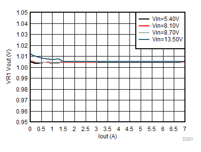
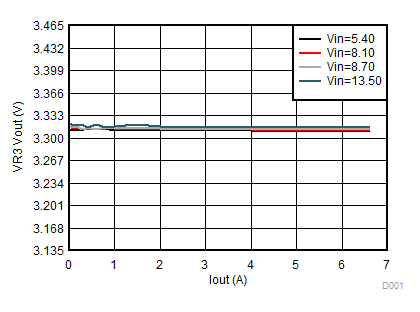
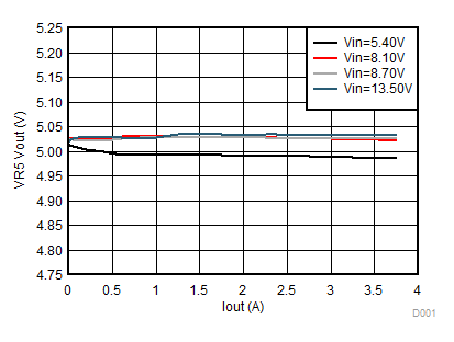
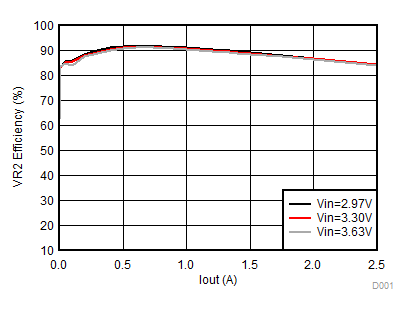
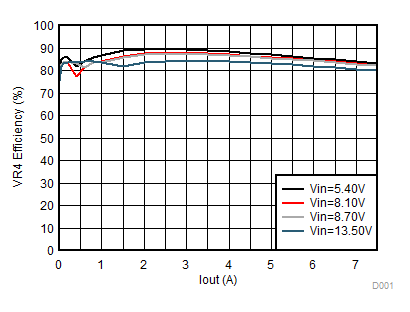
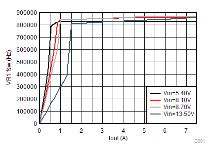
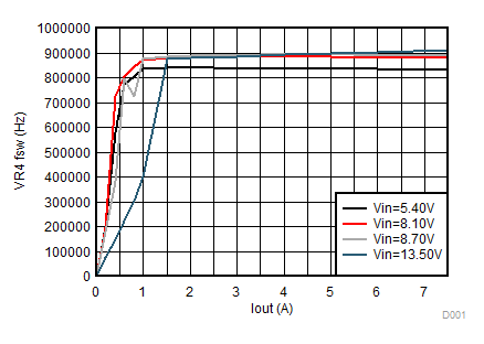
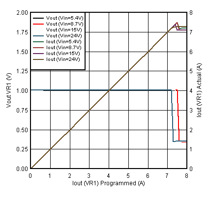 Figure 5-16 VR1 Current Limit: Vout and Iout vs Load, Non-NVDC
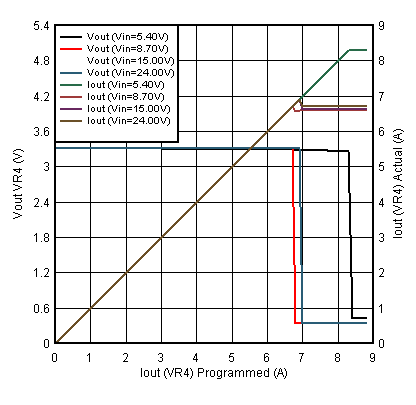 Figure 5-18 VR3 Current Limit: Vout and Iout vs Load, Non-NVDC
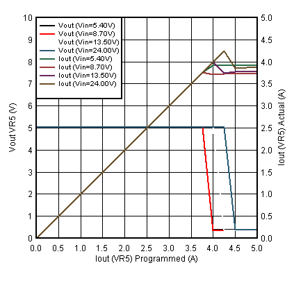 Figure 5-20 VR5 Current Limit: Vout and Iout vs Load, Non-NVDC
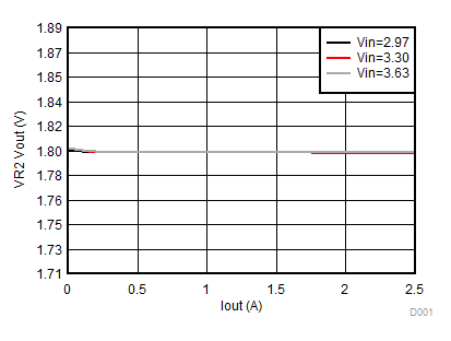
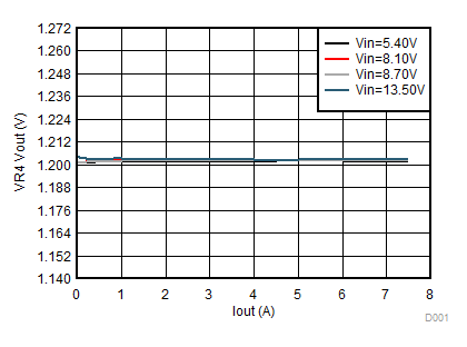
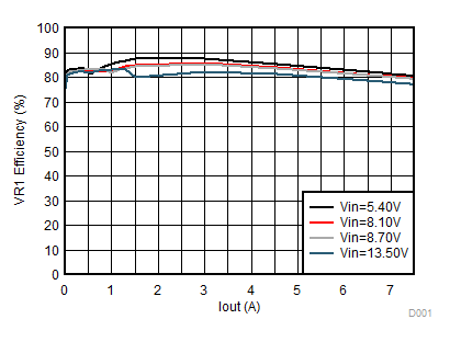
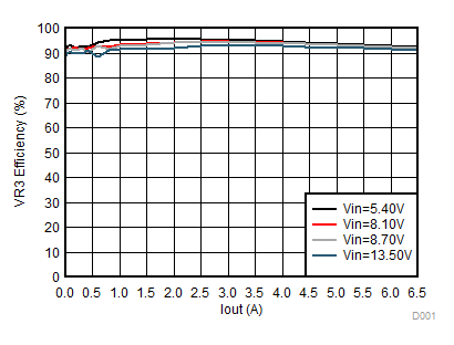

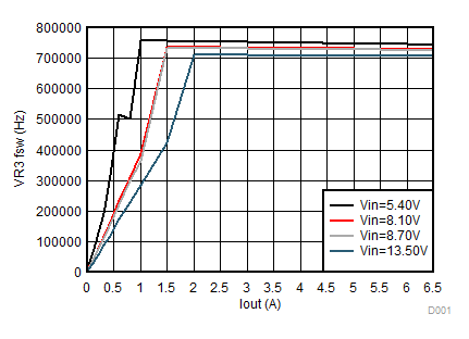
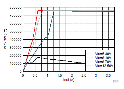
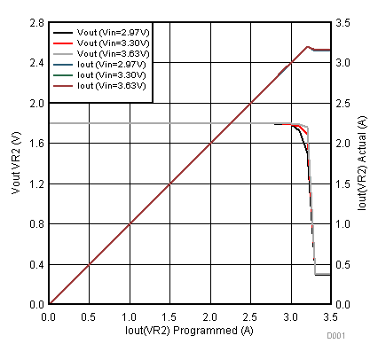 Figure 5-17 VR2 Current Limit: Vout and Iout vs Load, Non-NVDC
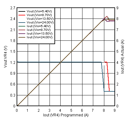 Figure 5-19 VR4 Current Limit: Vout and Iout vs Load, Non-NVDC
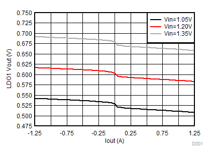
| Positive current = sinking from load. | ||
| Negative current = sourcing to load. | ||
| Inherent droop reduces transient ripple response | ||
