SLVS849C July 2008 – September 2017 TPS65100-Q1
PRODUCTION DATA.
- 1 Features
- 2 Applications
- 3 Description
- 4 Revision History
- 5 Pin Configuration and Functions
- 6 Specifications
- 7 Detailed Description
-
8 Application and Implementation
- 8.1 Application Information
- 8.2
Typical Applications
- 8.2.1
Supply for a Typical Approximately 7-inch Display
- 8.2.1.1 Design Requirements
- 8.2.1.2
Detailed Design Procedure
- 8.2.1.2.1
Boost Converter Design Procedure
- 8.2.1.2.1.1 Inductor Selection
- 8.2.1.2.1.2 Output Capacitor Selection
- 8.2.1.2.1.3 Input Capacitor Selection
- 8.2.1.2.1.4 Rectifier Diode Selection
- 8.2.1.2.1.5 Converter Loop Design and Stability
- 8.2.1.2.1.6 Design Procedure Quick Steps
- 8.2.1.2.1.7 Setting the Output Voltage and Selecting the Feedforward Capacitor
- 8.2.1.2.2 Negative Charge Pump
- 8.2.1.2.3 Positive Charge Pump
- 8.2.1.2.4 VCOM Buffer
- 8.2.1.2.5 Linear Regulator Controller
- 8.2.1.2.1
Boost Converter Design Procedure
- 8.2.1.3 Application Curves
- 8.2.2 Supply for a Typical Approximately 8-inch Display
- 8.2.1
Supply for a Typical Approximately 7-inch Display
- 9 Power Supply Recommendations
- 10Layout
- 11Device and Documentation Support
- 12Mechanical, Packaging, and Orderable Information
Package Options
Mechanical Data (Package|Pins)
- PWP|24
Thermal pad, mechanical data (Package|Pins)
- PWP|24
Orderable Information
8 Application and Implementation
NOTE
Information in the following applications sections is not part of the TI component specification, and TI does not warrant its accuracy or completeness. TI’s customers are responsible for determining suitability of components for their purposes. Customers should validate and test their design implementation to confirm system functionality.
8.1 Application Information
Figure 3 shows a general overview of the device and connections used in an application. Ranges are shown for several parameters to demonstrate the flexibility available to the application designer.
 Figure 3. Simplified Schematic
8.2 Typical Applications
8.2.1 Supply for a Typical Approximately 7-inch Display
A typical application requirement is to boost a 3.3-V or 5-V input to a 10-V, 13.5-V, or 15-V output. The Detailed Design Procedure section explains the step-by-step development.
 Figure 4. Supply for a 7-inch Display Diagram
8.2.1.1 Design Requirements
For this design example, use the parameters listed in Table 1 as the input parameters.
Table 1. Design Parameters
| DESIGN PARAMETER | EXAMPLE VALUE |
|---|---|
| VI | 3.3 V |
| VO1 | 10 V |
| VO2 | –5 V |
| VO3 | 23 V |
| Switch voltage drop, VSW | 0.5 V |
| Schottky diode forward voltage, VD | 0.8 V |
| VCOM | 5 V |
8.2.1.2 Detailed Design Procedure
8.2.1.2.1 Boost Converter Design Procedure
The first step in the design procedure is to calculate the maximum possible output current of the main boost converter under certain input and output voltage conditions. This example is for a 3.3-V to 10-V conversion:
- Duty cycle
- Average inductor current
- Inductor peak-to-peak ripple current
- Peak switch current


The integrated switch, the inductor, and the external Schottky diode must be able to handle the peak switch current. The calculated peak switch current must be equal to or lower than the minimum N-MOSFET switch current limit specified in Electrical Characteristics. If the peak switch current is higher, the converter cannot support the required load current. This calculation must be done for the minimum input voltage, where the peak switch current is highest. The calculation includes conduction losses like switch rDS(ON) (0.5 V) and diode forward drop voltage losses (0.8 V). Additional switching losses and inductor core and winding losses require a slightly higher peak switch current in the actual application. This calculation still allows for good design and component selection.
8.2.1.2.1.1 Inductor Selection
Several inductors work with the TPS65100-Q1 device and, particularly with the external compensation, performance can be adjusted to application requirements. The main parameter for inductor selection is the saturation current of the inductor, which should be higher than the peak switch current as previously calculated, with additional margin to allow for heavy load transients and extreme start-up conditions. Another method is to choose an inductor with a saturation current at least as high as the minimum switch current limit of 1.6 A. The different switch-current limits allow selection of a physically smaller inductor when less output current is required. Another important parameter is inductor DC resistance. Usually, the lower the DC resistance, the higher the efficiency. However, inductor DC resistance is not the only parameter determining the efficiency. Especially for a boost converter where the inductor is the energy storage element, the type and material of the inductor influences the efficiency as well. At the high switching frequency of 1.6 MHz, inductor core losses, proximity effects, and skin effects are more important. Usually, an inductor with a larger form factor yields higher efficiency. The efficiency difference between different inductors can vary between 2% to 10%. TI recommends inductor values between 3.3 μH and 6.8 μH.
8.2.1.2.1.2 Output Capacitor Selection
For the best output voltage filtering, TI recommends a low ESR output capacitor. Ceramic capacitors have a low ESR value, but depending on the application, tantalum capacitors can be used as well. A 22-μF ceramic output capacitor works for most of the applications. Higher capacitor values can be used to improve the load transient regulation. The output voltage ripple can be calculated as:

where
- IP = Peak switch current as calculated in the previous section with ISW(peak)
- L = Selected inductor value
- IO = Normal load current
- ƒS = Switching frequency
- VD = Rectifier diode forward voltage (typical 0.3 V)
- CO = Selected output capacitor
- ESR = Output capacitor ESR value
8.2.1.2.1.3 Input Capacitor Selection
For good input voltage filtering, TI recommends low ESR ceramic capacitors. A 22-μF ceramic input capacitor is sufficient for most of the applications. For better input voltage filtering, this value can be increased.
8.2.1.2.1.4 Rectifier Diode Selection
To achieve high efficiency, a Schottky diode should be used. The voltage rating must be higher than the maximum output voltage of the converter. The average forward current must be equal to the average inductor current of the converter. The main parameter influencing the efficiency of the converter is the forward voltage and the reverse leakage current of the diode; both must be as low as possible.
8.2.1.2.1.5 Converter Loop Design and Stability
The TPS65100-Q1 device converter loop can be externally compensated and allows access to the internal transconductance error amplifier output at the COMP pin. A small feedforward capacitor across the upper feedback resistor divider speeds up the circuit as well. To test the converter stability and load transient performance of the converter, a load step from 50 mA to 250 mA is applied, and the output voltage of the converter is monitored. Applying load steps to the converter output is a good tool to judge the stability of such a boost converter.
8.2.1.2.1.6 Design Procedure Quick Steps
- Select the feedback resistor divider to set the output voltage.
- Select the feedforward capacitor to place a zero at 50 kHz.
- Select the compensation capacitor on pin COMP. The smaller the value, the higher the low frequency gain.
- Use a 50-kΩ potentiometer in series to CC and monitor VO1 during load transients. Fine tune the load transient by adjusting the potentiometer. Select a resistor value that comes closest to the potentiometer resistor value. This needs to be done at the highest VI and highest load current since the stability is most critical at these conditions.
8.2.1.2.1.7 Setting the Output Voltage and Selecting the Feedforward Capacitor
The output voltage is set by the external resistor divider and is calculated as:

Across the upper resistor a bypass capacitor is required to speed up the circuit during load transients as shown in Figure 5.
Together with R1 the bypass capacitor C8 sets a zero in the control loop at approximately 50 kHz:

A value closest to the calculated value should be used. Larger feedforward capacitor values reduce the load regulation of the converter and cause load steps as shown in Figure 6.
 Figure 6. Load Step Caused By A Too Large Feed-forward Capacitor Value
For more information on how to calculate a Boost Converter's Output Stage refer to Basic Calculation of a Boost Converter's Power Stage.
8.2.1.2.2 Negative Charge Pump
The negative charge pump provides a regulated output voltage by inverting the main output voltage VO1. The negative charge pump output voltage within its output voltage range is set with external feedback resistors.
The maximum load current of the negative charge pump depends on the voltage drop across the external Schottky diodes and the internal on resistance of the charge pump MOSFETS. When the voltage drop across these components is larger than the voltage difference from VO1 to VO2, the charge pump is in dropout, providing the maximum possible output current. Therefore, the higher the voltage difference between VO1 and VO2, the higher the possible load current. See Figure 16 for the possible output current versus boost converter voltage VO1.
Estimating the maximum output voltage range of a single negative charge-pump stage:
Setting the output voltage:


The lower feedback resistor value R4 should be in a range between 40 kΩ to 120 kΩ or the overall feedback resistance should be within 500 kΩ to 1 MΩ. Smaller values load the reference too heavily and larger values may cause stability problems. For this design, 619 kΩ and 150 kΩ were chosen, delivering –5 V. The negative charge pump requires two external-Schottky diodes. The peak current rating of the Schottky diode has to be twice the load current of the output. For a 20-mA output current, the dual Schottky diode BAT54 or similar is a good choice.
8.2.1.2.3 Positive Charge Pump
The positive charge pump can be operated in a voltage doubler mode or a voltage tripler mode.
The output voltage needs to be within the voltage ranges of the configuration, see Voltage Doubler Mode and Voltage Tripler Mode. The output voltage within its limitation is set by the external resistor divider and is calculated as:


The maximum load current of the positive charge pump depends on the voltage drop across the internal Schottky diodes, the internal ON-resistance of the charge pump MOSFETS, and the impedance of the flying capacitor. When the voltage drop across these components is larger than the voltage difference VO1 × 2 to VO3 (doubler mode) or VO1 × 3 to VO3 (tripler mode), then the charge pump is in dropout, providing the maximum possible output current. Therefore, the higher the voltage difference between VO1 x 2 (doubler) or VO1 × 3 (tripler) to VO3, the higher the possible load current. See Figure 17 and Figure 18 for output current versus boost converter voltage, VO1, and the following calculations.
8.2.1.2.3.1 Voltage Doubler Mode
- Leave C2+ pin open
- Connect C2–/Mode to GND
The following shows first order formulas to calculate the minimum and maximum output voltages of the positive charge pump in doubler mode
- Minimum: VO3min = VO1
- Maximum: VO3max = 2 × VO1 – (2 VF + 2 × IO × (2 × rDS(on)Q5 + rDS(on)Q3 + rDS(on)Q4))
For detailed information how to estimate the output voltage ranges refer to How to Estimate the Output Voltage Range of the Charge Pumps in the TPS6510x and TPS6514x. SLVA918
8.2.1.2.3.2 Voltage Tripler Mode
- Connect flying capacitor to C2+ and C2–/MODE
The following shows first order formulas to calculate the minimum and maximum output voltages of the positive charge pump in doubler mode
- Minimum: VO3min = 2 × VO1 – (2 VF + 2 × IO × (2 × rDS(on)Q5 + rDS(on)Q3 + rDS(on)Q4))
- Maximum: VO3max = 3 × VO1 – (4 × VF + 2 × IO × (3 × rDS(on)Q5 + rDS(on)Q3 + rDS(on)Q4 ))
For detailed information how to estimate the output voltage ranges refer to How to Estimate the Output Voltage Range of the Charge Pumps in the TPS6510x and TPS6514x SLVA918.
8.2.1.2.4 VCOM Buffer
The VCOM buffer is typically used to drive the backplane of a TFT panel. The VCOM output voltage is typically set to half of the main output voltage VO1 plus a small shift to implement the specific compensation voltage. The TFT video signal gets coupled through the TFT storage capacitor plus the LCD cell capacitance to the output of the VCOM buffer. Because of these, short current pulses in the positive and negative direction appear at the output of the VCOM buffer. To minimize the output voltage ripple caused by the current pulses, a transconductance amplifier having a current source output and an output capacitor is used. The output capacitor supports the high frequency part of the current pulses drawn from the LCD panel. The VCOM buffer only needs to handle the low frequency portion of the current pulses. A 1-μF ceramic output capacitor is sufficient for most of the applications. When using other output capacitor values it is important to keep in mind that the output capacitor is part of the VCOM buffer loop stabilization.
The VCOM buffer has an integrated soft start to avoid voltage drops on VO1 during start-up. The soft start is implemented as such that the VCOMIN is held low until the VCOM buffer is fully biased and the common mode range is reached. Then the positive input is released and the VCOM buffer output slowly comes up. Usually a 1-nF capacitor on VCOMIN to GND is used to filter high frequency noise coupled in from VO1. The size of this capacitor together with the upper feedback resistor value determines the start-up time. The larger the capacitor from VCOMIN to GND, the slower the soft start.
8.2.1.2.5 Linear Regulator Controller
The TPS65100-Q1 device includes a linear regulator controller to generate a 3.3-V rail when the system is powered from a 5-V supply. Because an external NPN transistor is required, the input voltage of the TPS65100-Q1 device applied to VIN needs to be higher than the output voltage of the regulator. To provide a minimum base drive current of 13.5 mA, a minimum internal voltage drop of 500 mV from VI to Vbase is required. This can be translated into a minimum input voltage on VI for a certain output voltage as Equation 13 shows:
The current design operating from VI = 3.3 V cannot support this and the linear regulator is not used. The second example operating from VI = 5 V has the 3.3-V regulator implemented.
The base drive current together with the hFE of the external transistor determines the possible output current. External transistors are selected depending on the output current, power dissipation, and PCB space requirements of the application. The device is stable with a 4.7-μF ceramic output capacitor. Larger output capacitor values can be used to improve the load transient response when higher load currents are required.
8.2.1.3 Application Curves
Table 2. Table Of Graphs
| FIGURE | ||
|---|---|---|
| Main Boost Converter | ||
| Efficiency VO1 | vs Load current | Figure 7 |
| Efficiency VO1 | vs Load current | Figure 8 |
| Efficiency VO1 | vs Input voltage | Figure 9 |
| PWM operation, continuous mode | Figure 10 | |
| PWM operation at light load | Figure 11 | |
| Load transient response, CO = 22 μF | Figure 12 | |
| Load transient response, CO = 2 × 22 μF | Figure 13 | |
| Power-up sequencing | Figure 14 | |
| Soft start VO1 | Figure 15 | |
| Negative Charge Pump | ||
| VO2 Maximum load current | vs Output voltage VO1 | Figure 16 |
| Positive Charge Pump | ||
| VO3 Maximum load current | vs Output voltage VO1 (doubler mode) | Figure 17 |
| VO3 Maximum load current | vs Output voltage VO1 (tripler mode) | Figure 18 |
 Figure 7. Efficiency VO1 vs Load Current
 Figure 9. Efficiency VO1 vs Input Voltage
 Figure 11. PWM Operation At Light Load
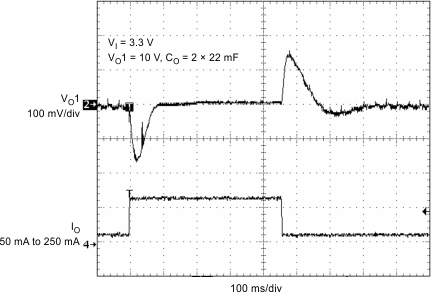 Figure 13. Load Transient Response 2 x CO
 Figure 15. Soft Start VO1
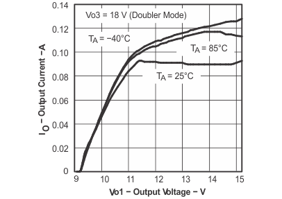 Figure 17. VO3 Maximum Load Current (Doubler Mode)
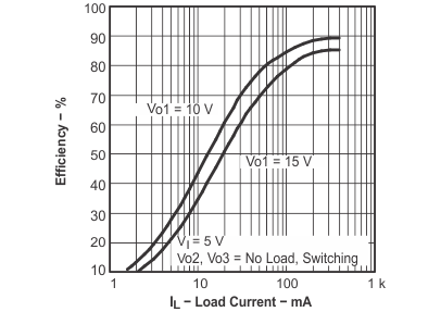 Figure 8. Efficiency VO1 vs Load Current
 Figure 10. PWM Operation Continuous Mode
 Figure 12. Load Transient Response 1 x CO
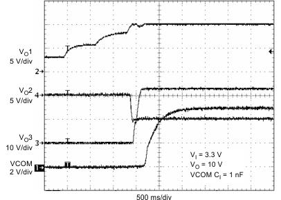 Figure 14. Power-Up Sequencing
 Figure 16. VO2 Maximum Load Current
 Figure 18. VO3 Maximum Load Current (Tripler Mode)
8.2.2 Supply for a Typical Approximately 8-inch Display
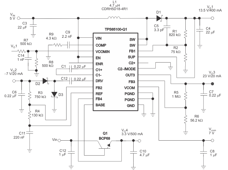 Figure 19. Simplified Schematic for a Typical Approximately 8-inch Display
