SLVSBB2F May 2012 – August 2024 TPS65131-Q1
PRODUCTION DATA
- 1
- 1 Features
- 2 Applications
- 3 Description
- 4 Device Comparison
- 5 Pin Configuration and Functions
- 6 Specifications
- 7 Detailed Description
-
8 Application and Implementation
- 8.1 Application Information
- 8.2
Typical Applications
- 8.2.1 TPS65131-Q1 With VPOS = 10.5V, VNEG = –10V
- 8.2.2 Design Requirements
- 8.2.3 Detailed Design Procedure
- 8.2.4 Analog Supply Input Filter
- 8.2.5 Thermal Information
- 8.2.6 Application Curves
- 8.3 Power Supply Recommendations
- 8.4 Layout
- 9 Device and Documentation Support
- 10Revision History
- 11Mechanical, Packaging, and Orderable Information
Package Options
Mechanical Data (Package|Pins)
- RGE|24
Thermal pad, mechanical data (Package|Pins)
- RGE|24
Orderable Information
3 Description
The TPS65131-Q1 device is dual-output dc-dc converter generating a positive output voltage up to 15V and a negative output voltage down to –15V with output currents of typically 200mA, depending on input-voltage to output-voltage ratio. With a total efficiency up to 85%, the device is ideal for portable battery-powered equipment. The input-voltage range of 2.7V to 5.5V allows, for example, 3.3V and 5V rails to power the TPS65131-Q1 device. The TPS65131-Q1 device comes in a QFN-24 package with thermal pad and wettable flanks. Requiring few and small external components, the overall solution size can be small.
The converter operates with a fixed-frequency PWM control topology and, with power-save mode enabled, uses a pulse-skipping mode at light load currents. In operation, the typical overall device quiescent current is only 500µA. In shutdown, the device draws typically 0.2µA. Independent enable pins allow power-up and power-down sequencing for both outputs. The device has an internal current limit, overvoltage protection, and a thermal shutdown for highest reliability under fault conditions.
The TPS65131-Q1 device is qualified for automotive applications, according to AEC-Q100 temperature grade 2. The electrical characteristics are tested over –40°C to 125°C device junction temperature. This, combined with lowest shutdown currents, small solution size, package with thermal pad, plus good efficiency and protection features, targets automotive and industrial applications.
| PART NUMBER | PACKAGE | BODY SIZE (NOM) |
|---|---|---|
| TPS65131-Q1 | VQFN (24) | 4mm × 4mm |
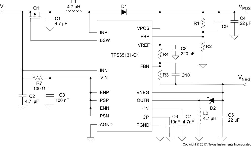
 Application Schematic