SLVS497F SEPTEMBER 2003 – June 2016 TPS65140 , TPS65141 , TPS65145
PRODUCTION DATA.
- 1 Features
- 2 Applications
- 3 Description
- 4 Revision History
- 5 Pin Configuration and Functions
- 6 Specifications
- 7 Detailed Description
-
8 Application and Implementation
- 8.1 Application Information
- 8.2
Typical Application
- 8.2.1 Design Requirements
- 8.2.2
Detailed Design Procedure
- 8.2.2.1
Boost Converter Design Procedure
- 8.2.2.1.1 Inductor Selection
- 8.2.2.1.2 Output Capacitor Selection
- 8.2.2.1.3 Input Capacitor Selection
- 8.2.2.1.4 Rectifier Diode Selection
- 8.2.2.1.5 Converter Loop Design and Stability
- 8.2.2.1.6 Design Procedure Quick Steps
- 8.2.2.1.7 Setting the Output Voltage and Selecting the Feedforward Capacitor
- 8.2.2.1.8 Compensation
- 8.2.2.1.9 Negative Charge Pump
- 8.2.2.1.10 Positive Charge Pump
- 8.2.2.1.11 Linear Regulator Controller
- 8.2.2.1
Boost Converter Design Procedure
- 8.2.3 Application Curves
- 8.3 System Examples
- 9 Power Supply Recommendations
- 10Layout
- 11Device and Documentation Support
- 12Mechanical, Packaging, and Orderable Information
Package Options
Refer to the PDF data sheet for device specific package drawings
Mechanical Data (Package|Pins)
- RGE|24
- PWP|24
Thermal pad, mechanical data (Package|Pins)
Orderable Information
8 Application and Implementation
NOTE
Information in the following applications sections is not part of the TI component specification, and TI does not warrant its accuracy or completeness. TI’s customers are responsible for determining suitability of components for their purposes. Customers should validate and test their design implementation to confirm system functionality.
8.1 Application Information
The TPS6514x devices have been designed to provide the input supply voltages for the source drivers and gate drivers in LCD displays. Additionally, they include a linear regulator controller that can be used with an external transistor to provide a regulated 3.3-V output for the digital circuits for LCD panels powered by a 5-V supply rail.
8.2 Typical Application
Figure 3 shows a typical application circuit for a monitor display powered from a 5-V supply. It generates up to 350 mA at 15 V to power the source drivers, and 20 mA at 30 V and –12 V to power the gate drivers.
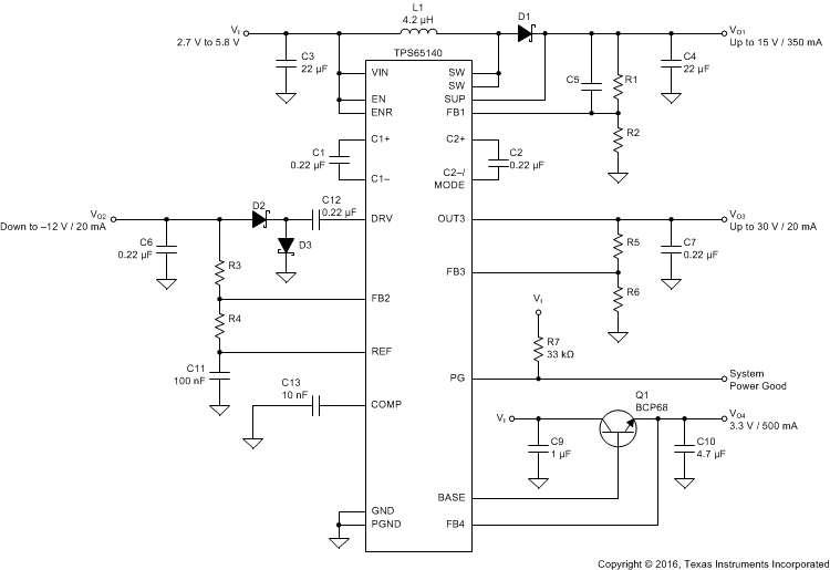 Figure 3. Typical Application Schematic
8.2.1 Design Requirements
Table 1 shows the design parameters for this example.
Table 1. Design Requirements
| PARAMETER | VALUE | |
|---|---|---|
| VI | Input supply voltage | 2.7 V to 5.8 V |
| VO1 | Boost converter output voltage and current | Up to 15 V at 350 mA |
| VO3 | Positive charge pump output voltage and current | Up to 30 V at 20 mA |
| VO2 | Negative charge pump output voltage and current | Down to –12 V at 20 mA |
| VO4 | Linear regulator controller output voltage and current | 3.3 V at 500 mA |
8.2.2 Detailed Design Procedure
8.2.2.1 Boost Converter Design Procedure
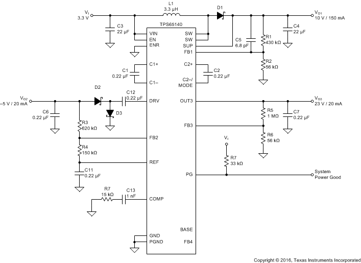
The first step in the design procedure is to calculate the maximum possible output current of the main boost converter under certain input and output voltage conditions. The following is an example for a 3.3-V to 10-V conversion:
VIN = 3.3 V, VOUT = 10 V, Switch voltage drop VSW = 0.5 V, Schottky diode forward voltage VD = 0.8 V
- Duty cycle:
- Average inductor current:
- Inductor peak-to-peak ripple current:
- Peak switch current:


The integrated switch, the inductor, and the external Schottky diode must be able to handle the peak switch current. The calculated peak switch current must be equal to or lower than the minimum N-MOSFET switch current limit as specified in Electrical Characteristics (1.6 A for the TPS65140 and TPS65141 and 0.96 A for the TPS65145). If the peak switch current is higher, then the converter cannot support the required load current. This calculation must be done for the minimum input voltage where the peak switch current is highest. The calculation includes conduction losses like switch rDS(on) (0.5 V) and diode forward drop voltage losses (0.8 V). Additional switching losses, inductor core and winding losses, and so forth, require a slightly higher peak switch current in the actual application. The above calculation still allows for a good design and component selection.
8.2.2.1.1 Inductor Selection
Several inductors work with the TPS6514x. Especially with the external compensation, the performance can be adjusted to the specific application requirements. The main parameter for the inductor selection is the saturation current of the inductor which must be higher than the peak switch current as calculated above with additional margin to cover for heavy load transients and extreme start-up conditions. Another method is to choose the inductor with a saturation current at least as high as the minimum switch current limit of 1.6 A for the TPS65140 and TPS65141 and 0.96 A for the TPS65145. The different switch current limits allow selection of a physically smaller inductor when less output current is required. The second important parameter is the inductor DC resistance. Usually, the lower the DC resistance, the higher the efficiency. However, the inductor DC resistance is not the only parameter determining the efficiency. Especially for a boost converter where the inductor is the energy storage element, the type and material of the inductor influences the efficiency as well. Especially at high switching frequencies of 1.6 MHz, inductor core losses, proximity effects, and skin effects become more important. Usually, an inductor with a larger form factor yields higher efficiency. The efficiency difference between different inductors can vary from 2% to 10%. For the TPS6514x, inductor values from 3.3 µH to 6.8 µH are a good choice but other values can be used as well. Possible inductors are shown in Table 2.
Table 2. Inductor Selection
| DEVICE | INDUCTOR VALUE | COMPONENT SUPPLIER | DIMENSIONS / mm | ISAT/DCR |
|---|---|---|---|---|
| TPS65140 | 4.7 µH | Coilcraft DO1813P-472HC | 8.89 × 6.1 × 5 | 2.6 A, 54 mΩ |
| 4.2 µH | Sumida CDRH5D28 4R2 | 5.7 × 5.7 × 3 | 2.2 A, 23 mΩ | |
| 4.7 µH | Sumida CDC5D23 4R7 | 6 × 6 × 2.5 | 1.6 A, 48 mΩ | |
| 3.3 µH | Wuerth Elektronik 744042003 | 4.8 × 4.8 × 2 | 1.8 A, 65 mΩ | |
| 4.2 µH | Sumida CDRH6D12 4R2 | 6.5 × 6.5 × 1.5 | 1.8 A, 60 mΩ | |
| 3.3 µH | Sumida CDRH6D12 3R3 | 6.5 × 6.5 × 1.5 | 1.9 A, 50 mΩ | |
| TPS65145 | 3.3 µH | Sumida CDPH4D19 3R3 | 5.1 × 5.1 × 2 | 1.5 A, 26 mΩ |
| 3.3 µH | Coilcraft DO1606T-332 | 6.5 × 5.2 × 2 | 1.4 A, 120 mΩ | |
| 3.3 µH | Sumida CDRH2D18/HP 3R3 | 3.2 × 3.2 × 2 | 1.45 A, 69 mΩ | |
| 4.7 µH | Wuerth Elektronik 744010004 | 5.5 × 3.5 × 1 | 1 A, 260 mΩ | |
| 3.3 µH | Coilcraft LPO6610-332M | 6.6 × 5.5 × 1 | 1.3 A, 160 mΩ |
8.2.2.1.2 Output Capacitor Selection
For best output voltage filtering, TI recommends a low-ESR output capacitor. Ceramic capacitors have a low ESR value but depending on the application, tantalum capacitors can be used as well. A 22-µF ceramic output capacitor works for most of the applications. Higher capacitor values can be used to improve load transient regulation. See Table 2 for the selection of the output capacitor. The output voltage ripple can be calculated as:

where
- IP = Peak switch current as calculated in the previous section with ISW(peak)
- L = Selected inductor value
- IOUT = Normal load current
- fS = Switching frequency
- VD = Rectifier diode forward voltage (typical 0.3 V)
- COUT = Selected output capacitor
- ESR = Output capacitor ESR value
8.2.2.1.3 Input Capacitor Selection
For good input voltage filtering, TI recommends low-ESR ceramic capacitors. A 22-µF ceramic input capacitor is sufficient for most of applications. For better input voltage filtering, this value can be increased. See Table 3 and the typical applications for input capacitor recommendations.
Table 3. Input and Output Capacitors Selection
| CAPACITOR | VOLTAGE RATING | COMPONENT SUPPLIER | COMMENTS |
|---|---|---|---|
| 22 µF, 1210 | 16 V | Taiyo Yuden EMK325BY226MM | CO |
| 22 µF, 1206 | 6.3 V | Taiyo Yuden JMK316BJ226 | CI |
8.2.2.1.4 Rectifier Diode Selection
To achieve high efficiency, a Schottky diode must be used. The voltage rating must be higher than the maximum output voltage of the converter. The average forward current must be equal to the average inductor current of the converter. The main parameter influencing the efficiency of the converter is the forward voltage and the reverse leakage current of the diode; both must be as low as possible. Possible diodes are: On Semiconductor MBRM120L, Microsemi UPS120E, and Fairchild Semiconductor MBRS130L.
8.2.2.1.5 Converter Loop Design and Stability
The TPS6514x converter loop can be externally compensated and allows access to the internal transconductance error amplifier output at the COMP pin. A small feedforward capacitor across the upper feedback resistor divider speeds up the circuit as well. To test the converter stability and load transient performance of the converter, a load step from 50 mA to 250 mA is applied, and the output voltage of the converter is monitored. Applying load steps to the converter output is a good tool to judge the stability of such a boost converter.
8.2.2.1.6 Design Procedure Quick Steps
- Select the feedback resistor divider to set the output voltage.
- Select the feedforward capacitor to place a zero at 50 kHz.
- Select the compensation capacitor on pin COMP. The smaller the value, the higher the low frequency gain.
- Use a 50-kΩ potentiometer in series to CC and monitor VOUT during load transients. Fine tune the load transient by adjusting the potentiometer. Select a resistor value that comes closest to the potentiometer resistor value. This must be done at the highest Vin and highest load current because stability is most critical at these conditions.
8.2.2.1.7 Setting the Output Voltage and Selecting the Feedforward Capacitor
The output voltage is set by the external resistor divider and is calculated as:

Across the upper resistor, a bypass capacitor is required to speed up the circuit during load transients as shown in Figure 4.
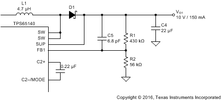 Figure 4. Feedforward Capacitor
Together with R1 the bypass capacitor C8 sets a zero in the control loop at approximately 50 kHz:

A value closest to the calculated value must be used. Larger feedforward capacitor values reduce the load regulation of the converter and cause load steps as shown in Figure 5.
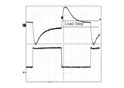 Figure 5. Load Step Caused by a Too Large Feedforward Capacitor Value
8.2.2.1.8 Compensation
The regulator loop can be compensated by adjusting the external components connected to the COMP pin. The COMP pin is connected to the output of the internal transconductance error amplifier. A typical compensation scheme is shown in Figure 6.
 Figure 6. Compensation Network
The compensation capacitor CC adjusts the low frequency gain, and the resistor value adjusts the high frequency gain. The following formula calculates at what frequency the resistor increases the high frequency gain.

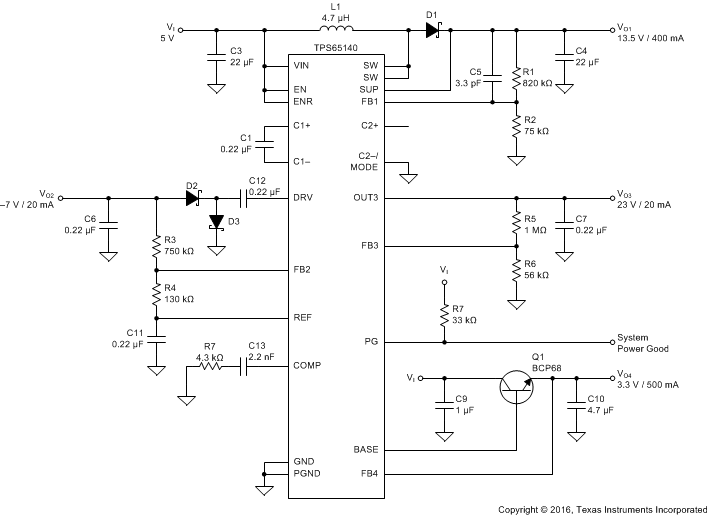
Lower input voltages require a higher gain and a lower compensation capacitor value. A good start is CC = 1 nF for a 3.3-V input and CC = 2.2 nF for a 5-V input. If the device operates over the entire input voltage range from 2.7 V to 5.8 V, TI recommends a larger compensation capacitor up to 10 nF. Figure 7 shows the load transient with a larger compensation capacitor, and Figure 8 shows a smaller compensation capacitor.
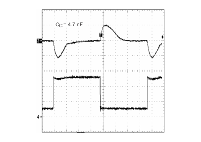 Figure 7. CC = 4.7 nF
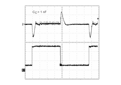 Figure 8. CC = 1 nF
Lastly, RC must be selected. A good practice is to use a 50-kΩ potentiometer and adjust the potentiometer for the best load transient where no oscillations should occur. These tests have to be done at the highest VIN and highest load current because the converter stability is most critical under these conditions. Figure 9, Figure 10, and Figure 11 show the fine tuning of the loop with RC.
 Figure 9. Overcompensated (Damped Oscillation),
RC is Too Large
 Figure 11. Optimum, RC is Ideal
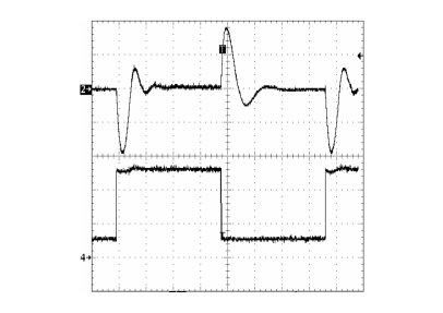 Figure 10. Undercompensated (Loop is Too Slow),
RC is Too Small
8.2.2.1.9 Negative Charge Pump
The negative charge pump provides a regulated output voltage by inverting the main output voltage, VO1. The negative charge pump output voltage is set with external feedback resistors.
The maximum load current of the negative charge pump depends on the voltage drop across the external Schottky diodes, the internal ON-resistance of the charge pump MOSFETS Q8 and Q9, and the impedance of the flying capacitor, C12. When the voltage drop across these components is larger than the voltage difference from VO1 to VO2, the charge pump is in drop out, providing the maximum possible output current. Therefore, the higher the voltage difference between VO1 and VO2, the higher the possible load current. See Figure 21 for the possible output current versus boost converter voltage VO1 and the calculations below.
Setting the output voltage:


The lower feedback resistor value, R4, must be in a range from 40 kΩ to 120 kΩ or the overall feedback resistance must be within 500 kΩ to 1 MΩ. Smaller values load the reference too heavy and larger values may cause stability problems. The negative charge pump requires two external Schottky diodes. The peak current rating of the Schottky diode must be twice the load current of the output. For a 20-mA output current, the dual Schottky diode BAT54 or similar is a good choice.
8.2.2.1.10 Positive Charge Pump
The positive charge pump can be operated in a voltage doubler mode or a voltage tripler mode depending on the configuration of the C2+ and C2–/MODE pins. Leaving the C2+ pin open and connecting C2-/MODE to GND forces the positive charge pump to operate in a voltage doubler mode. If higher output voltages are required the positive charge pump can be operated as a voltage tripler. To operate the charge pump in the voltage tripler mode, a flying capacitor must be connected to C2+ and C2–/MODE.
The maximum load current of the positive charge pump depends on the voltage drop across the internal Schottky diodes, the internal ON-resistance of the charge pump MOSFETS, and the impedance of the flying capacitor. When the voltage drop across these components is larger than the voltage difference VO1 × 2 to VO3 (doubler mode) or VO1 × 3 to VO3 (tripler mode), then the charge pump is in dropout, providing the maximum possible output current. Therefore, the higher the voltage difference between VO1 x 2 (doubler) or VO1 × 3 (tripler) to VO3, the higher the possible load current. See Figure 22 and Figure 23 for output current versus boost converter voltage, VO1, and the following calculations.
Voltage doubler:
Voltage tripler:
The output voltage is set by the external resistor divider and is calculated as:


8.2.2.1.11 Linear Regulator Controller
The TPS6514x includes a linear regulator controller to generate a 3.3-V rail when the system is powered from a 5-V supply. Because an external NPN transistor is required, the input voltage of the TPS6514x applied to VIN must be higher than the output voltage of the regulator. To provide a minimum base drive current of 13.5 mA, a minimum internal voltage drop of 500 mV from VI to VBASE is required. This can be translated into a minimum input voltage on VIN for a certain output voltage as the following calculation shows:
The base drive current together with the hFE of the external transistor determines the possible output current. Using a standard NPN transistor like the BCP68 allows an output current of 1 A and using the BCP54 allows a load current of 337 mA for an input voltage of 5 V. Other transistors can be used as well, depending on the required output current, power dissipation, and PCB space. The device is stable with a 4.7-µF ceramic output capacitor. Larger output capacitor values can be used to improve the load transient response when higher load currents are required.
8.2.3 Application Curves
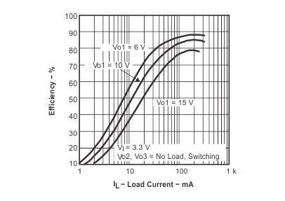 Figure 12. Efficiency vs Load Current
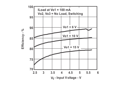 Figure 14. Efficiency vs Input Voltage
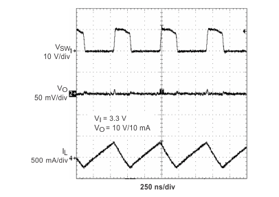 Figure 16. PWM Operation at Light Load
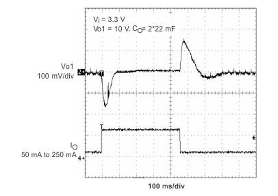 Figure 18. Load Transient Response
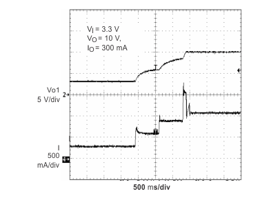 Figure 20. Soft Start VO1
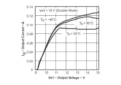 Figure 22. VO3 Maximum Load Current
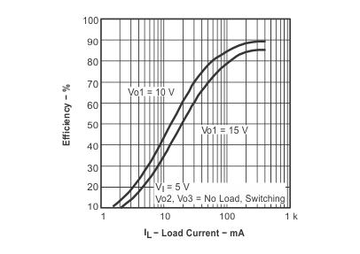 Figure 13. Efficiency vs Load Current
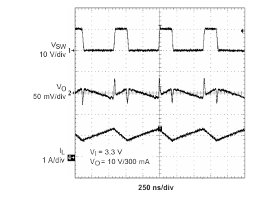 Figure 15. PWM Operation Continuous Mode
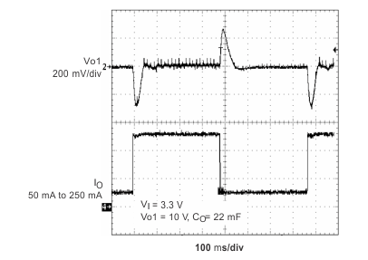 Figure 17. Load Transient Response
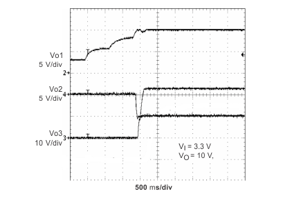 Figure 19. Power-Up Sequencing
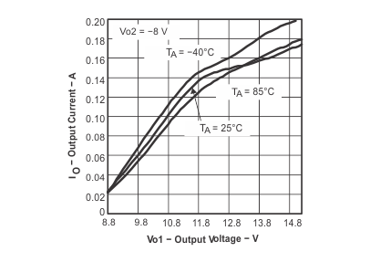 Figure 21. VO2 Maximum Load Current
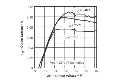 Figure 23. VO3 Maximum Load Current
