SLVSAX5B July 2011 – August 2015 TPS65142
PRODUCTION DATA.
- 1 Features
- 2 Applications
- 3 Description
- 4 Revision History
- 5 Pin Configuration and Functions
- 6 Specifications
-
7 Detailed Description
- 7.1 Overview
- 7.2 Functional Block Diagram
- 7.3
Feature Description
- 7.3.1 AVDD Boost Regulator
- 7.3.2 Regulated Positive Charge Pump
- 7.3.3 Negative Charge Pump
- 7.3.4 Gate Voltage Shaping
- 7.3.5 VCOM Buffer
- 7.3.6 Reset
- 7.3.7 Under-voltage Lockout (UVLO)
- 7.3.8 Thermal Shutdown
- 7.3.9 WLED Boost Regulator
- 7.3.10 Current Sinks
- 7.3.11 Unused IFB Pins
- 7.3.12 PWM Dimming
- 7.3.13 Enabling the WLED Driver
- 7.3.14 Soft-Start of WLED Boost Regulator
- 7.3.15 Protection of WLED Driver
- 7.3.16 Power Up/Down Sequence
- 8 Application and Implementation
- 9 Device and Documentation Support
- 10Mechanical, Packaging, and Orderable Information
Package Options
Mechanical Data (Package|Pins)
- RTG|32
Thermal pad, mechanical data (Package|Pins)
- RTG|32
Orderable Information
7 Detailed Description
7.1 Overview
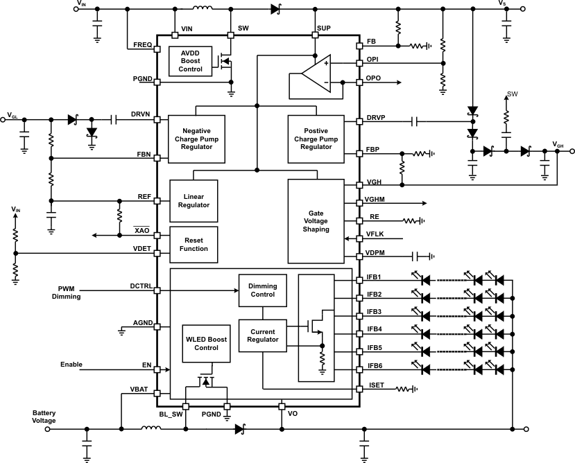
The TPS65142 offers a compact and complete solution to the bias power and the WLED backlight in note-pc TFT-LCD panels. The device features an AVDD boost regulator, a positive charge pump regulator, and a negative charge pump regulator to power the source drivers and the gate drivers. A 150-mA unity-gain high-speed buffer is provided to drive the VCOM plane. Gate voltage shaping and the LCD discharge function are offered to improve the image quality. A reset function allows a proper reset of the TCON at power on or the gate driver ICs during power off. The TPS65142 also includes the complete solution to drive up to 6 chains of WLEDs with 1000:1 ratio PWM dimming.
7.2 Functional Block Diagram
7.3 Feature Description
7.3.1 AVDD Boost Regulator
The AVDD boost regulator is designed for output voltages up to 16.5 V with a switch peak current limit of 1.8 A minimum. The device, which operates in a current-mode scheme with quasi-constant frequency, is internally compensated to minimize the pin and component counts. The switching frequency is selectable between 650 kHz and 1.2 MHz and the minimum input voltage is 2.3 V.
During the on-time, the current rises in the inductor. When the current reaches a threshold value set by the internal GM amplifier, the power transistor is turned off. The polarity of the inductor voltage changes and forward biases the Schottky diode, which lets the current flow towards the output of the boost regulator. The off-time is fixed for a certain input voltage VIN and output voltage VS, and therefore maintains the same frequency when varying these parameters. However, for different output loads, the frequency changes slightly due to the voltage drop across the rDS(on) of the power transistor which will have an effect on the voltage across the inductor and thus on tON (tOFF remains fixed).
The fixed off-time maintains a quasi-fixed frequency that provides better stability for the system over a wide range of input and output voltages than conventional boost converters. The TPS65142 topology has also the benefits of providing very good load and line regulations, and excellent line and load transient responses.
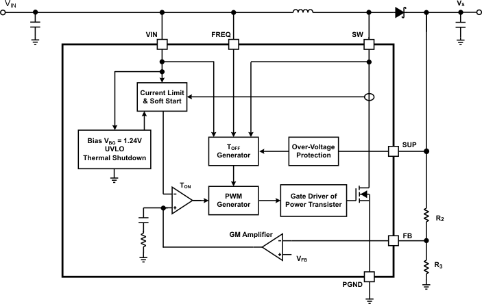 Figure 25. Boost Converter Block Diagram
7.3.1.1 Setting the Output Voltage
The output voltage is set by an external resistor divider. Typically, a minimum current of 50 µA flowing through the feedback divider is enough to cover the noise fluctuation. If 70 µA is chosen for higher noise immunity, the resistors shown in Figure 25 are then calculated as:

where VFBP = 1.240 V
7.3.1.2 Soft-Start (AVDD Boost Converter)
The AVDD boost converter has an internal digital soft-start to prevent high inrush current during start-up. The typical soft-start time is 2 ms.
7.3.1.3 Frequency Select Pin (FREQ)
The digital frequency-select pin FREQ allows to set the switching frequency of the device to 650 kHz (FREQ = low) or 1.2 MHz (FREQ = high). Higher switching frequency improves load transient response but reduces slightly the efficiency. The other benefit of a higher switching frequency is the lower output voltage ripple. Usually, it is recommended to use 1.2-MHz switching frequency unless light load efficiency is a major concern.
7.3.1.4 Overvoltage Protection
The AVDD boost converter has an integrated over-voltage protection to prevent the power switch from exceeding the absolute maximum switch voltage rating at pin SW in case the feedback (FB) pin is floating or shorted to GND. In such an event, the output voltage rises and is monitored with the overvoltage protection comparator over the SUP pin. As soon as the comparator trips at typically 18 V, the boost converter turns the N-Channel MOSFET switch off. The output voltage falls below the overvoltage threshold and the converter continues to operate. In order to detect overvoltage, the SUP pin must to be connected to the output voltage of the boost converter VS.
7.3.2 Regulated Positive Charge Pump
The positive charge pump sets the voltage applied on the VGH input pin, up to 32 V in tripler mode configuration. The charge pump block regulates the VGH voltage by adjusting the drive current IDRVP. Typically, a minimum current of 50 µA flowing through the feedback divider is usually enough to cover the noise fluctuation. If 70 µA is chosen for higher noise immunity, the resistors of the divider used to set the VGH voltage are calculated as (refer to Figure 26):

where VFBP = 1.240 V
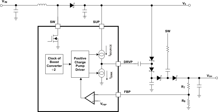 Figure 26. Block Diagram of the Positive Charge Pump Regulator
7.3.3 Negative Charge Pump
Figure 27 shows the block diagram of the negative charge pump. The negative charge pump needs to generate a voltage of –6 V to –7 V with a negative inverter or –12 V to –13 V with a negative doubler. The reference voltage from the REF pin is 3.15 V. The bias to the REF block comes from the SUP pin. The error amplifier is referenced to the ground. The VGL can be set with the following equation:

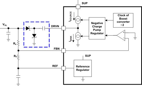 Figure 27. Block Diagram of the Negative Charge Pump Regulator with a Negative Inverter Configuration
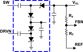 Figure 28. Negative Doubler Configuration for the Negative Charge Pump Regulator
7.3.4 Gate Voltage Shaping
The VGHM output is controlled by the VFLK logic input and the VDPM voltage level.
The VDPM pin allows the user to set a delay before the Gate Voltage Shaping starts. The voltage of the VDPM pin is zero volt at power on. When the output voltage of the AVDD boost converter rises above a power-good threshold, a power-good signal enables a 20-µA current source that charges the capacitor connected between the VDPM pin and the ground. When the VDPM-pin voltage rises to 1.24 V, the Gate Voltage Shaping is enabled.
The VFLK input controls the M1 and the M2 transistors, as shown in Figure 29, after the Gate Voltage Shaping is enabled:
When VFLK = “low”, M1 is turned on so VGHM is connected to the VGH input.
When VFLK = “high”, M2 is turned on so VGHM voltage is discharged through M2 and the resistor connected to the RE pin.
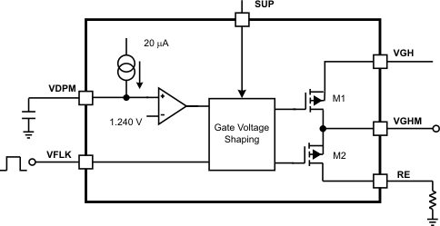 Figure 29. Block Diagram of the Gate Voltage Shaping Function
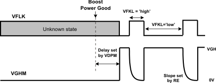 Figure 30. Gate Voltage Shaping Timing
7.3.5 VCOM Buffer
The VCOM Buffer power supply pin is the SUP pin connected to the AVDD boost converter VS. To achieve good performance and minimize the output noise, a 1-µF ceramic bypass capacitor is required directly from the SUP pin to ground. The buffer is not designed to drive high capacitive loads; therefore, it is recommended to connect a series resistor at the output to provide stable operation when driving a high capacitive load. With a 3.3-Ω series resistor, a capacitive load of 10 nF can be driven, which is usually sufficient for typical LCD applications.
7.3.6 Reset
The device has an integrated reset function with an open-drain output capable of sinking 1 mA. The reset function monitors the voltage applied to its sense input V(DET). As soon as the voltage on V(DET) falls below the threshold voltage, V(DET), of typically 1.1 V, the reset function asserts its reset signal by pulling XAO low. Typically, a minimum current of 50 µA flowing through the feedback divider is enough to cover the noise fluctuation. Therefore, to select R12 and R13 (see Figure 33), one has to set the input voltage limit (VIN(LIM)) at which the reset function will pull XAO to low state. VIN(LIM) must be higher than the UVLO threshold. If 70 µA is chosen,

where VDET = 1.1 V.
The XAO output is also controlled by the UVLO function. When the input voltage is below the UVLO threshold, XAO output is forced low until the input voltage is lower than 1.6 V. The XAO output is in an unknown state when the input voltage is below the 1.6 V threshold.
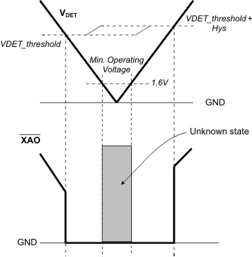 Figure 31. Voltage Detection and XAO Pin
When the input voltage VIN rises, once the voltage on VDET pin exceeds its threshold voltage plus the hysteresis, the XAO signal will go high.
The reset function is operational for VIN ≥ 1.6 V.
The reset function is configured as a standard open-drain and requires a pull-up resistor. The resistor R(XAO) (R14 in Figure 33), which must be connected between the XAO pin output and a positive voltage VX greater than 2 V – 'high' logic level can be chosen as follows:

7.3.7 Under-voltage Lockout (UVLO)
The TPS65142 monitors both VIN and VBAT inputs for under-voltage lockout. When the VIN input in under its UVLO threshold, the whole IC is disabled to avoid mis-operation. When the VIN input rises above its UVLO threshold, all functions are enabled except the WLED driver. The WLED driver, including the WLED boost converter and the current sinks, will be enabled when the VBAT input is also higher than its UVLO threshold.
7.3.8 Thermal Shutdown
A thermal shutdown is implemented to prevent damages because of excessive heat and power dissipation. Typically the thermal shutdown threshold for the junction temperature is 150°C. When the thermal shutdown is triggered the device stops switching until the junction temperature falls below typically 136°C. Then the device starts switching again.
7.3.9 WLED Boost Regulator
The WLED boost regulator is a current-mode PWM regulator with internal loop compensation. The internal compensation ensures a stable output over the full input and output voltage range. The WLED boost regulator switches at fixed 1 MHz. The output voltage of the boost regulator is automatically set by the TPS65142 to minimize the voltage drop across the current-sink IFBx pins. The lowest IFB-pin voltage to regulated to 400 mV. When the output voltage is too close to the input, the WLED boost regulator may not be able to regulate the output due to the limitation of the minimum duty cycle. In that case, the user needs to increase the number of WLED in series or to include series ballast resistors to provide enough headroom for the boost converter to operate. The WLED boost regulator cannot regulate its output to a voltage below 15 V.
7.3.10 Current Sinks
The six current sink regulators can each provide a maximum of 25 mA. The IFB current must be programmed to the highest WLED current expected using an ISET-pin resistor with the following equation:

where
K(ISET) = Current multiple (1000 typical)
V(ISET) = ISET pin voltage (1.229 V typical)
R(ISET) = ISET-pin resistor value
The TPS65142 has built-in precise current sink regulators. The current matching error among 6 current sinks is below 2.5%. This means the differential values between the maximum and minimum currents of the six current sinks divided by the average current of the six is less than 2.5%.
7.3.11 Unused IFB Pins
If the application requires less than 6 WLED strings, one can easily disable unused IFBx pins by simply leaving the unused IFB pin open or shorting it to ground. If the IFB pin is open, the boost output voltage ramps up to VO overvoltage threshold during start up. The IC then detects the zero current string and removes it from the feedback loop. If the IFB pin is shorted to ground, the IC detects the short immediately after WLED driver is enable, and the boost output voltage does not go up to VO overvoltage threshold. Instead, it ramps to the regulation voltage after the soft start.
7.3.12 PWM Dimming
The WLED brightness is controlled by the PWM signal on the DCTRL pin. The frequency and duty cycle of the DCTRL signal is replicated on the IFB pin current. Keep the dimming frequency in the range of 100 Hz to 1 kHz to avoid screen flickering and to maintain dimming linearity. Screen flickering may occur if the dimming frequency is below the range. The minimum achievable duty cycle increases with the dimming frequency. For example, while a 0.1% dimming duty cycle, giving a 1000:1 dimming range, is achievable at 100 Hz dimming frequency, only 1% duty cycle, giving a 100:1 dimming range, is achievable with a 1-kHz dimming frequency, and 5% dimming duty cycle is achievable with 5 kHz dimming frequency. The device can work at high dimming frequency such as 20 kHz, but then only 15% duty cycle can be achieved. The TPS65142 is designed to minimize the AC ripple on the output capacitor during PWM dimming. Careful passive component selection is also critical to minimize AC ripple on the output capacitor.
7.3.13 Enabling the WLED Driver
The WLED driver (including the WLED boost converter and the six current sinks) is enabled when all following four conditions are satisfied:
- the VBAT input voltage is higher than its under-voltage-lockout (UVLO) threshold;
- the REF regulator output is higher than its power-good threshold;
- the output voltage VO is within 2 V of the input voltage VBAT;
- and the enable input from the EN pin is high.
Pulling the EN pin low shuts down the WLED driver.
7.3.14 Soft-Start of WLED Boost Regulator
Once the above four conditions are satisfied, the WLED boost converter begins the internal soft-start. The soft-start function gradually ramps up the reference voltage of the error amplifier to prevent the output-voltage over shoot and inrush current from the VBAT input.
7.3.15 Protection of WLED Driver
The TPS65142 has multiple protection mechanisms to secure the safe operation of the WLED driver.
7.3.15.1 Current Limit Protection
The WLED boost regulator switching MOSFET has a pulse-by-pulse over-current limit of 1.5 A (minimum value). The PWM switch turns off when the inductor current reaches this current threshold and remains off until the beginning of the next switching cycle. This protects the device and external components under over-load conditions. When there is sustained overcurrent condition for more than 16 ms (under 100% dimming duty cycle), the IC turns off and requires VBAT POR or the EN pin toggling to restart.
Under severe over load and/or short-circuit conditions, the VO pin can be pulled below the input (VBAT pin voltage). Under this condition, the current can flow directly from the input to the output through the inductor and the Schottky diode. Turning off the PWM switch alone does not limit current anymore. In this case, the TPS65142 relies on the fuse at the input to protect the whole system. When the TPS65142 detects the output voltage to be 1 V (short-circuit detection threshold) below the input voltage, it shuts down the WLED driver. The IC restarts after input power-on reset (VBAT POR) or EN pin logic toggling.
7.3.15.2 Open WLED String Protection
If one of the WLED strings is open, the boost output rises to its over-voltage threshold (39 V typically). The IC detects the open WLED string by sensing no current in the corresponding IFBx pin. As a result, the IC removes the open IFBx pin from the voltage feedback loop. The output voltage drops and is regulated to the voltage for the remaining connected WLED strings. The IFBx current of the connected WLED string remains in regulation during the whole transition.
The IC shuts down if it detects that all of the WLED strings are open.
7.3.15.3 Overvoltage Protection
If the overvoltage threshold is reached, but the current sensed on the IFBx pin is below the regulation target, the IC regulates the boost output at the overvoltage threshold. This operation could occur when the WLED is turned on under cold temperature, and the forward voltages of the WLEDs exceed the over-voltage threshold. Maintaining the WLED current allows the WLED to warm up and their forward voltages to drop below the overvoltage threshold.
If any IFBx pin voltage exceeds IFB overvoltage threshold (17 V typical), the IC turns off the corresponding current sink and removes this IFB pin from VO regulation loop. The remaining IFBx pins’ current regulation is not affected. This condition often occurs when there are several shorted WLEDs in one string. WLED mismatch typically does not create such large voltage difference among WLED strings.
7.3.16 Power Up/Down Sequence
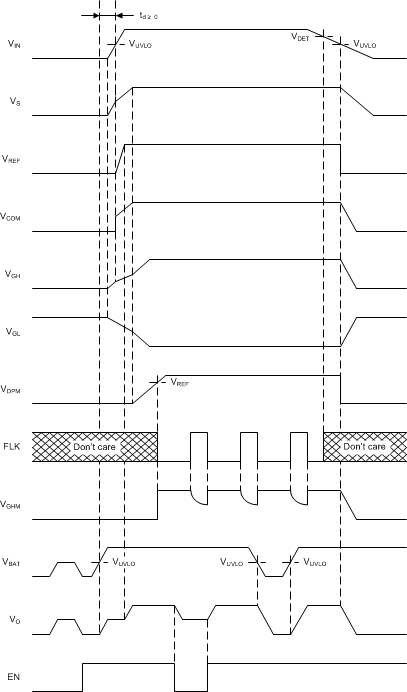
The power up and power down sequences are shown in Figure 32.
The operation of the bias converters are gated by the UVLO of the VIN voltage. The start-up of the WLED boost converter is gated by the UVLO of the VBAT input, the power good of the REF output, the (VBAT – 2 V) and VO comparator output, and the EN input. The REF output is powered by the output of the AVDD boost converter through the SUP pin; and hence, the WLED boost converter will not start before the AVDD boost converter.
7.3.16.1 Power Up Sequence
The power up sequence of the bias portion is as following. When the VIN rises above the ULVO threshold, and the internal device enable signal is asserted. The AVDD boost converter begins the soft-start, the REF regulator starts to rise, the VCOM buffer is enabled, and both charge pumps begins to operate. When the REF output reaches its regulation voltage, a VREF power good signal is asserted for the WLED section. The AVDD boost converter continues the soft start until its output voltage reaches the AVDD power good threshold when an AVDD power good signal is asserted. The AVDD power good signal enables the 20-µA current to the VDPM pin to start the gate voltage shaping delay timer. The delay is programmed by the external capacitor connected to the VDPM pin and should be long enough to ensure that both charge pumps are ready before the delay ends. Once the delay ends, the gate voltage shaping (VGHM) output is enabled to be controlled by the VFLK input.
The power up sequence of the WLED driver section is as following. When the four conditions for the Enabling the WLED Driver section are satisfied, the WLED boost converter begins the soft start, together with the start of the current sinks. When any of the four conditions is not satisfied, the WLED boost converter will stop switching.
To ensure proper start-up of the TPS65142 device, it is recommended to apply VBAT before VIN (see Timing Requirements and Figure 32).
7.3.16.2 Power Down Sequence and LCD Discharge Function
The power down sequence of the bias section is as following. When the input voltage VIN falls below a predefined threshold set by V(DET_THRESHOLD), XAO is driven low and the VGHM output is driven to VGH. (Note that when VIN falls below the UVLO threshold, all IC functions are disabled except XAO and VGHM outputs). Since VGHM is connected to VGH, it tracks the output of the positive charge pump as it decays. This feature, together with XAO, can be used to discharge the panel by turning on all the pixel TFTs and discharging them into the gradually decaying VGHM voltage. VHGM is held low during power-up.
The REF regulator will be disabled when VIN falls below the UVLO threshold, hence, the WLED boost converter as well.
