SLVSBG2A September   2013  – June 2016 TPS65154

PRODUCTION DATA.  

  1. Device Overview
    1. 1.1 Features
    2. 1.2 Applications
    3. 1.3 Description
    4. 1.4 Simplified System Diagram
  2. Revision History
  3. Pin Configuration and Functions
  4. Specifications
    1. 4.1 Absolute Maximum Ratings
    2. 4.2 ESD Ratings
    3. 4.3 Recommended Operating Conditions
    4. 4.4 Thermal Information
    5. 4.5 Electrical Characteristics
    6. 4.6 Timing Requirements
  5. Detailed Description
    1. 5.1 Overview
    2. 5.2 Functional Block Diagram
    3. 5.3 Feature Description
      1. 5.3.1  Linear Regulator (VCC)
        1. 5.3.1.1 Power-Up (Linear Regulator)
        2. 5.3.1.2 Power-Down (Linear Regulator)
        3. 5.3.1.3 Protection (Linear Regulator)
      2. 5.3.2  Boost Converter 1 (AVDD)
        1. 5.3.2.1 Power-Up (Boost Converter 1)
        2. 5.3.2.2 Power-Down (Boost Converter 1)
        3. 5.3.2.3 Protection (Boost Converter 1)
      3. 5.3.3  Boost Converter 2 (VGH)
        1. 5.3.3.1 Power-Up (Boost Converter 2)
        2. 5.3.3.2 Power-Down (Boost Converter 2)
        3. 5.3.3.3 Protection (Boost Converter 2)
      4. 5.3.4  Negative Charge Pump (VGL)
        1. 5.3.4.1 Power-Up (Negative Charge Pump)
        2. 5.3.4.2 Power-Down (Negative Charge Pump)
        3. 5.3.4.3 Protection (Negative Charge Pump)
      5. 5.3.5  Gate Voltage Shaping
      6. 5.3.6  Panel Discharge (XAO)
      7. 5.3.7  Reset Generator (RST)
      8. 5.3.8  Programmable VCOM
        1. 5.3.8.1 Operational Amplifier Performance
        2. 5.3.8.2 Power-Up (Programmable VCOM)
        3. 5.3.8.3 Power-Down (Programmable VCOM)
      9. 5.3.9  WLED Driver
        1. 5.3.9.1 WLED Boost Converter
        2. 5.3.9.2 Current Sinks
        3. 5.3.9.3 Protection
        4. 5.3.9.4 Enable and Start-Up
      10. 5.3.10 Undervoltage Lockout
    4. 5.4 Device Functional Modes
      1. 5.4.1 Dimming Modes
        1. 5.4.1.1 Direct Dimming
        2. 5.4.1.2 Phase-Shift Dimming
      2. 5.4.2 Power Sequencing
        1. 5.4.2.1 Power-Up
        2. 5.4.2.2 Power-Down
    5. 5.5 Programming
      1. 5.5.1 Configuration
        1. 5.5.1.1 General
          1. 5.5.1.1.1 I2C Interface
          2. 5.5.1.1.2 Slave Addresses
          3. 5.5.1.1.3 Write Protect
      2. 5.5.2 Programming Examples (Excluding VCOM)
        1. 5.5.2.1 Writing to a Single RAM Register
        2. 5.5.2.2 Writing to Multiple RAM Registers
        3. 5.5.2.3 Saving Contents of all RAM Registers to EEPROM
        4. 5.5.2.4 Reading from a Single RAM Register
        5. 5.5.2.5 Reading from a Single EEPROM Register
        6. 5.5.2.6 Reading from Multiple RAM Registers
        7. 5.5.2.7 Reading from Multiple EEPROM Registers
      3. 5.5.3 Programming Examples - VCOM
        1. 5.5.3.1 Writing a VCOM Value of 77h to WR
        2. 5.5.3.2 Writing a VCOM Value of 77h to IVR and WR
        3. 5.5.3.3 Reading a VCOM Value of 77h from WR
        4. 5.5.3.4 Reading a VCOM Value of 77h from IVR
    6. 5.6 Register Map
      1. 5.6.1 Configuration Registers (Excluding VCOM)
        1. 5.6.1.1  CONFIG (00h)
        2. 5.6.1.2  VCC (01h)
        3. 5.6.1.3  DLY1 (02h)
        4. 5.6.1.4  AVDD (03h)
        5. 5.6.1.5  FSW1 (04h)
        6. 5.6.1.6  SS2 (05h)
        7. 5.6.1.7  DLY2 (06h)
        8. 5.6.1.8  VGL (07h)
        9. 5.6.1.9  SS3 (08h)
        10. 5.6.1.10 DLY3 (09h)
        11. 5.6.1.11 VGH (0Ah)
        12. 5.6.1.12 SS4 (0Bh)
        13. 5.6.1.13 FSW3 (0Ch)
        14. 5.6.1.14 DLY4 (0Dh)
        15. 5.6.1.15 OVP (0Eh)
        16. 5.6.1.16 FDIM (OFh)
        17. 5.6.1.17 RESET (10h)
        18. 5.6.1.18 VDET (11h)
        19. 5.6.1.19 DLY6 (12h)
        20. 5.6.1.20 VMAX (13h)
        21. 5.6.1.21 VMIN (14h)
        22. 5.6.1.22 USER (15h)
        23. 5.6.1.23 CONTROL (FFh)
      2. 5.6.2 VCOM Registers
        1. 5.6.2.1 VCOM DATA (Slave Address 28h, Register Address 00h)
        2. 5.6.2.2 VCOM CONTROL (Slave Address 28h, Register Address 02h)
  6. Application and Implementation
    1. 6.1 Application Information
    2. 6.2 Typical Application
      1. 6.2.1 Design Requirements
      2. 6.2.2 Detailed Design Procedure
        1. 6.2.2.1 External Component Selection
      3. 6.2.3 Application Curves
  7. Power Supply Recommendations
  8. Layout
    1. 8.1 Layout Guidelines
    2. 8.2 Layout Example
  9. Device and Documentation Support
    1. 9.1 Device Support
      1. 9.1.1 Third-Party Products Disclaimer
    2. 9.2 Receiving Notification of Documentation Updates
    3. 9.3 Community Resources
    4. 9.4 Trademarks
    5. 9.5 Electrostatic Discharge Caution
    6. 9.6 Glossary
  10. 10Mechanical, Packaging, and Orderable Information
    1. 10.1 Packaging Information

Package Options

Mechanical Data (Package|Pins)
Thermal pad, mechanical data (Package|Pins)
Orderable Information

1 Device Overview

1.1 Features

  • 2.0 V to 5.5 V Input Voltage Range
  • Synchronous Boost Converter (AVDD)
  • Non-Synchronous Boost Converter (VGH)
  • Low Dropout Linear Regulator (VCC)
  • Programmable VCOM Calibrator with Integrated Buffer Amplifier
  • 6-Channel WLED Driver with Direct Dimming and Phase-Shift Dimming Modes
  • Gate Voltage Shaping
  • Panel Reset Signal (XAO)
  • T-CON Reset Signal (RST)
  • On-Chip EEPROM with Write Protect
  • I2C Interface
  • Thermal Shutdown
  • 48-Pin, 6 mm × 6 mm, 0.4 mm Pitch VQFN

1.2 Applications

  • Notebook PCs
  • Tablet PCs

1.3 Description

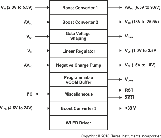
The TPS65154 is a compact LCD bias solution primarily intended for use in Notebook and Tablet PCs. The device comprises two boost converters to supply the LCD panel's source driver and gate driver; a linear regulator to supply the system's logic voltage; a programmable VCOM with high-speed amplifier; and a gate voltage shaping function; and a 6-channel WLED driver. 

spacing

Device Information(1)

PART NUMBER PACKAGE BODY SIZE (NOM)
TPS65154 VQFN (48) 6.00 mm × 6.0mm
(1) For all available packages, see the orderable addendum at the end of the data manual.

1.4 Simplified System Diagram
TPS65154 functional_block_diag_lvsbg2.gif