SLVSA76G March 2010 – January 2016 TPS65180B , TPS65181 , TPS65181B
PRODUCTION DATA.
- 1 Features
- 2 Applications
- 3 Description
- 4 Revision History
- 5 Description (continued)
- 6 Device Comparison Table
- 7 Pin Configuration and Functions
- 8 Specifications
-
9 Detailed Description
- 9.1 Overview
- 9.2 Functional Block Diagram
- 9.3 Feature Description
- 9.4 Device Functional Modes
- 9.5
Register Maps
- 9.5.1 Thermistor Readout (TMST_VALUE) Register (Offset = 0x00h)
- 9.5.2 Enable (ENABLE) Register (Offset = 0x01h)
- 9.5.3 Positive Voltage Rail Adjustment (VP_ADJUST) Register (Offset = 0x02h)
- 9.5.4 Negative Voltage Rail Adjustment (VN_ADJUST) Register (Offset = 0x03h)
- 9.5.5 VCOM Adjustment (VCOM_ADJUST) Register (Offset = 0x04h)
- 9.5.6 Interrupt Enable 1 (INT_ENABLE1) Register (Offset = 0x05h)
- 9.5.7 Interrupt Enable 2 (INT_ENABLE2) Register (Offset = 0x06h)
- 9.5.8 Interrupt INT_STATUS1 (INT_STATUS1) Register (Offset = 0x07h)
- 9.5.9 Interrupt Status 2 (INT_STATUS2) Register (Offset = 0x08h)
- 9.5.10 Power Sequence Register 0 (PWR_SEQ0) Register (Offset = 0x09h)
- 9.5.11 Power Sequence Register 1 (PWR_SEQ1) Register (Offset = 0x0Ah)
- 9.5.12 Power Sequence Register 2 (PWR_SEQ2) Register (Offset = 0x0Bh)
- 9.5.13 Thermistor Configuration Register (TMST_CONFIG) (Offset = 0x0Ch)
- 9.5.14 Thermistor Hot Threshold (TMST_OS) Register (Offset = 0x0Dh)
- 9.5.15 Thermistor Cool Threshold (TMST_HYST) Register (Offset = 0x0Eh)
- 9.5.16 Power-Good Status (PG_STATUS) Register (Offset = 0x0Fh)
- 9.5.17 Revision and Version Control (REVID) Register (Offset = 0x10h)
- 9.5.18 I2C Read Pointer Control (FIX_READ_POINTER) Register (Offset = 0x11h) (TPS65181 and TPS65181B ONLY)
-
10Application and Implementation
- 10.1
Application Information
- 10.1.1 Dependencies Between Rails
- 10.1.2 Soft-Start
- 10.1.3 VCOM Adjustment
- 10.1.4 VCOM Adjustment Through Register Control
- 10.1.5 VCOM Adjustment Through External Potentiometer
- 10.1.6 VPOS and VNEG Supply Tracking
- 10.1.7 Fault Handling and Recovery
- 10.1.8 TPS65180 and TPS65180B Fault Handling
- 10.1.9 TPS65181 and TPS65181B Fault Handling
- 10.1.10 Power-Good Pin
- 10.1.11 Interrupt Pin
- 10.1.12 Panel Temperature Monitoring
- 10.1.13 NTC Bias Circuit
- 10.1.14 TPS65180 and TPS65180B Temperature Acquisition
- 10.1.15 TPS65181 and TPS65181B Temperature Acquisition
- 10.1.16 Overtemperature Reporting
- 10.1.17 Overtemperature Fault Queuing
- 10.1.18 TPS65181 and TPS65181B Temperature Sensor
- 10.1.19 I2C Bus Operation
- 10.2 Typical Application
- 10.1
Application Information
- 11Power Supply Recommendations
- 12Layout
- 13Device and Documentation Support
- 14Mechanical, Packaging, and Orderable Information
Package Options
Mechanical Data (Package|Pins)
- RGZ|48
Thermal pad, mechanical data (Package|Pins)
- RGZ|48
Orderable Information
12 Layout
12.1 Layout Guidelines
The layout guidelines are listed as follows.
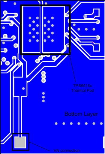
- PBKG die substrate must connect to VN (–16 V) with short, wide trace. Wide copper trace improves heat dissipation.
- The PowerPAD is internally connected to PBKG and must be connected to ground, but connected to VN with a short, wide copper trace.
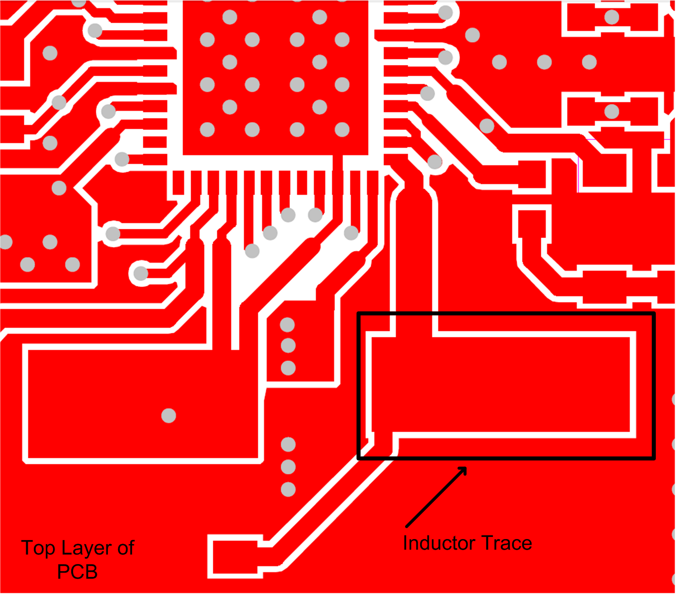
- Inductor traces must be kept on the PCB top layer free of any vias.
- Feedback traces must be routed away from any potential noise source to avoid coupling.
- Output caps must be placed immediately at output pin.
- VIN pins must be bypassed to ground with low-ESR ceramic bypass capacitors.
12.2 Layout Example
 Figure 17. Layout Top Layer
 Figure 18. Layout Bottom Layer