SLVSAQ8G February 2011 – September 2017 TPS65185
PRODUCTION DATA.
- 1 Features
- 2 Applications
- 3 Description
- 4 Revision History
- 5 Description (continued)
- 6 Pin Configuration and Functions
- 7 Specifications
-
8 Detailed Description
- 8.1 Overview
- 8.2 Functional Block Diagram
- 8.3
Feature Description
- 8.3.1 Wake-Up and Power-Up Sequencing
- 8.3.2 Dependencies Between Rails
- 8.3.3 Soft Start
- 8.3.4 Active Discharge
- 8.3.5 VPOS/VNEG Supply Tracking
- 8.3.6 V3P3 Power Switch
- 8.3.7 VCOM Adjustment
- 8.3.8 Fault Handling And Recovery
- 8.3.9 Power Good Pin
- 8.3.10 Interrupt Pin
- 8.3.11 Panel Temperature Monitoring
- 8.4 Device Functional Modes
- 8.5 Programming
- 8.6
Register Maps
- 8.6.1 Thermistor Readout (TMST_VALUE) Register (address = 0x00h) [reset = N/A]
- 8.6.2 Enable (ENABLE) Register (address = 0x01h) [reset = 0h]
- 8.6.3 Voltage Adjustment (VADJ) Register (address = 0x02h) [reset = 23h]
- 8.6.4 VCOM 1 (VCOM1) Register (address = 0x03h) [reset = 7Dh]
- 8.6.5 VCOM 2 (VCOM2) Register (address = 0x04h) [reset = 04h]
- 8.6.6 Interrupt Enable 1 (INT_EN1) Register (address = 0x05h) [reset = 7Fh]
- 8.6.7 Interrupt Enable 2 (INT_EN2) Register (address = 0x06h) [reset = FFh]
- 8.6.8 Interrupt 1 (INT1) Register (address = 0x07h) [reset = 0h]
- 8.6.9 Interrupt 2 (INT2) Register (address = 0x08h) [reset = N/A]
- 8.6.10 Power-Up Sequence 0 (UPSEQ0) Register (address = 0x09h) [reset = E4h]
- 8.6.11 Power-Up Sequence 1 (UPSEQ1) Register (address = 0x0Ah) [reset = 55h]
- 8.6.12 Power-Down Sequence 0 (DWNSEQ0) Register (address = 0x0Bh) [reset = 1Eh]
- 8.6.13 Power-Down Sequence 1 (DWNSEQ1) Register (address = 0x0Ch) [reset = E0h]
- 8.6.14 Thermistor 1 (TMST1) Register (address = 0x0Dh) [reset = 20h]
- 8.6.15 Thermistor 2 (TMST2) Register (address = 0x0Eh) [reset = 78h]
- 8.6.16 Power Good Status (PG) Register (address = 0x0Fh) [reset = 0h]
- 8.6.17 Revision and Version Control (REVID) Register (address = 0x10h) [reset = 45h]
- 9 Application and Implementation
- 10Power Supply Recommendations
- 11Layout
- 12Device and Documentation Support
- 13Mechanical, Packaging, and Orderable Information
Package Options
Mechanical Data (Package|Pins)
Thermal pad, mechanical data (Package|Pins)
Orderable Information
1 Features
- Single Chip Power-Management Solution for
E Ink® Vizplex™ Electronic Paper (E-Paper) Displays - Generates Positive and Negative Gates, and Source Driver Voltages and Back-Plane Bias From a Single, Low-Voltage Input Supply
- Supports 9.7-Inch and Larger Panel Sizes
- 3-V to 6-V Input Voltage Range
- Boost Converter for Positive Rail Base
- Inverting Buck-Boost Converter for Negative Rail Base
- Two Adjustable LDOs for Source Driver Supply
- Accurate Output Voltage Tracking
- VPOS – VNEG = ±50 mV
- Two Charge Pumps for Gate Driver Supply
- CP1: 22 V, 15 mA (VDDH)
- CP2: –20 V, 15 mA, (VEE)
- Adjustable VCOM Driver for Accurate Panel-Backplane Biasing
- 0 V to –5.11 V
- ± 1.5% accuracy (±10 mV)
- 9-Bit Control (10-mV Nominal Step Size)
- Active Discharge on All Rails
- Integrated 10-Ω, 3.3-V Power Switch for Disabling System Power Rail to E-Ink Panel
2 Applications
- Power Supply for Active Matrix E Ink Vizplex Panels
- Electronic Paper Display (EPD) Power Supplies
- E-Book Readers
- Dual-Display Phone and Tablets
- Application Processors With Integrated or Software Timing Controller (OMAP™)
3 Description
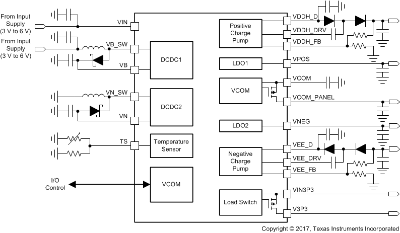
The TPS65185x device is a single-chip power supply designed to for E Ink Vizplex displays used in portable e-reader applications, and the device supports panel sizes up to 9.7 inches and greater. Two high efficiency DC-DC boost converters generate ±16-V rails that are boosted to 22 V and –20 V by two change pumps to provide the gate driver supply for the Vizplex panel. Two tracking LDOs create the ±15-V source driver supplies that support up to 120/200 mA (TPS65185/TPS651851) of output current. All rails are adjustable through the I2C interface to accommodate specific panel requirements.
Device Information(1)
| PART NUMBER | PACKAGE | BODY SIZE (NOM) |
|---|---|---|
| TPS65185 | RGZ (48) | 7.00 mm × 7.00 mm |
| RSL (48) | 6.00 mm × 6.00 mm | |
| TPS651851 | RSL (48) | 6.00 mm × 6.00 mm |
- For all available packages, see the orderable addendum at the end of the data sheet.
